

Maintaining material consistency in the production of bipolar-CMOS-DMOS (BCD) devices has become a central challenge for high-volume manufacturing (HVM) as the demand for integrated power management and digital control systems accelerates. While BCD technology serves as the backbone for critical applications—ranging from automotive safety systems to high-efficiency power electronics—the complexity of these devices requires unprecedented levels of process control. Achieving uniform device performance is no longer merely a function of electrical testing; it is a prerequisite established during the deposition phase of fabrication.
The transition toward more demanding end markets has necessitated a paradigm shift in how thin-film deposition is monitored. Silicon-Chromium (SiCr) films, which are instrumental in providing the resistance necessary for analog accuracy, are particularly sensitive to deposition conditions. Even subtle variations in gas flow or sputtering parameters can alter the microstructural integrity of these films. Consequently, manufacturers are increasingly adopting advanced, non-destructive metrology techniques to gain deeper visibility into process excursions before they manifest as failures in downstream assembly.
The Role of SiCr Films in BCD Technology
BCD technology is unique in its integration of bipolar, CMOS, and DMOS transistors on a single die. This architecture requires precise thin-film resistors, typically composed of SiCr, to ensure the stability of the analog signals that govern power conversion and sensor interfaces. In the contemporary semiconductor landscape, where power density and heat management are paramount, the thickness and composition of these resistors are critical variables.
Historically, thin-film metrology relied on secondary techniques that were either too slow for HVM or required destructive sampling. The industry has recently pivoted toward picosecond ultrasonic technology. This method utilizes laser-generated acoustic waves to probe the physical properties of films. By measuring the time-of-flight of acoustic echoes within the SiCr layer, engineers can determine film thickness with extreme precision. However, as process nodes shrink and performance requirements tighten, thickness measurements have proven to be an incomplete indicator of overall film quality.

Bridging the Gap: Beyond Thickness Measurements
While thickness uniformity is a fundamental metric for resistor matching, it does not account for variations in stoichiometry, density, or surface morphology. Two films may possess identical thicknesses yet exhibit vastly different electrical behaviors. This discrepancy is often rooted in the microstructure of the material—specifically, the grain size and the spacing between grain boundaries.
These microstructural attributes are heavily influenced by the sputtering environment, particularly the interaction between reactive gases (such as Nitrogen) and the target material. A shift in the nitrogen flow rate can lead to variations in the SiCr-nitride formation, which in turn alters the Temperature Coefficient of Resistance (TCR). Because TCR is a primary determinant of how a device performs under thermal stress, failing to detect these changes during the deposition phase can lead to significant yield loss.
The integration of reflectivity data into the existing picosecond ultrasonic platform provides a multi-dimensional view of the film. Reflectivity acts as a proxy for surface roughness and density. A smoother, denser film typically yields higher reflectivity, while a rougher, more porous surface results in lower reflectivity. By capturing this data simultaneously with acoustic thickness measurements, process engineers can distinguish between a nominal deposition process and one that is drifting toward an excursion, even if the film thickness remains within the target specification.
Chronology of Metrology Advancements in BCD
The evolution of metrology for SiCr deposition can be viewed through several distinct phases:
- Early Implementation (Pre-2015): Manufacturers primarily relied on electrical probing post-fabrication to identify resistors that fell outside of target resistance ranges. This resulted in high scrap rates and delayed failure detection.
- The Rise of In-Line Thickness Control (2015–2020): With the introduction of non-destructive optical and acoustic metrology, companies began measuring thickness directly on production wafers. This shift reduced the need for monitor wafers and improved throughput.
- The Modern Multimodal Era (2021–Present): Industry leaders are now adopting "simultaneous acquisition" strategies. By extracting both physical thickness and surface reflectivity in a single scan, fabs are achieving a holistic view of film health that correlates directly with the stoichiometry and grain structure of the SiCr film.
Analyzing the Impact of Gas Flow Variations
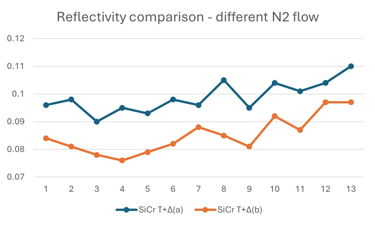
The influence of process variables on thin-film quality is best illustrated by the correlation between nitrogen (N2) flow and optical signatures. In controlled experiments conducted by applications engineers, wafers processed under two distinct nitrogen flow rates were compared.

In the higher-flow condition, the resulting SiCr film was observed to have a lower thickness but higher reflectivity. Conversely, the lower-flow condition resulted in a thicker film with lower reflectivity. These reflectivity signatures are indicative of how the gas flow affects the nucleation and growth of the SiCr film. Because the reflectivity measurement is collected simultaneously with the acoustic pulse-echo signal, there is no latency added to the metrology cycle. This is a crucial benefit for high-volume fabs where the "cost of measurement"—measured in time and throughput—is a significant component of the total cost of ownership.
Industry Implications and Future Outlook
The ability to identify process excursions in real-time has profound implications for the semiconductor industry, particularly for automotive and medical device manufacturers where the cost of failure is extreme. The "zero-defect" culture prevalent in the automotive sector demands that potential process variations are identified at the earliest possible stage.
By utilizing picosecond ultrasonic technology to monitor both thickness and reflectivity, manufacturers can establish more robust control limits. If a reflectivity signature drifts, engineers can adjust gas flow controllers or sputtering power before the excursion impacts the entire batch. This proactive approach to process control is expected to be a standard requirement as the industry moves toward 300mm wafer processing for power electronics.
"The goal is not just to measure the film, but to understand the health of the deposition process," notes a senior applications engineer involved in the research. "When we combine reflectivity with thickness, we aren’t just seeing a number; we are seeing a snapshot of the material’s structural integrity. This level of insight allows for the fine-tuning of sputtering recipes that were previously considered ‘black boxes’."
Broader Economic and Reliability Impacts
The economic impact of improved process control in BCD manufacturing is twofold. First, it directly contributes to higher yields. By reducing the number of wafers that must be discarded due to resistance mismatches, manufacturers can significantly lower their per-unit production costs. Second, it enhances the long-term reliability of the final products. In the automotive industry, where electronic control units (ECUs) are exposed to extreme temperature fluctuations, the stability of SiCr resistors is critical. A film with consistent microstructural properties is inherently more resistant to drift over the multi-year lifespan of a vehicle.

As BCD technology continues to scale, the industry must rely on metrology solutions that provide deeper, more granular data. The combination of picosecond acoustics and reflectivity is a testament to the shift toward intelligent, data-driven manufacturing. By leveraging the synergies between these two measurements, semiconductor facilities can maintain the rigorous standards required for modern electronics, ensuring that the devices powering our world are as reliable as they are precise.
In conclusion, the necessity for integrated, multi-modal metrology is clear. As manufacturers face the dual pressures of scaling production and maintaining high device performance, the use of picosecond ultrasonic technology stands out as a vital tool. By moving beyond simple thickness monitoring and incorporating qualitative indicators like reflectivity, the semiconductor industry is better equipped to navigate the complexities of thin-film deposition, thereby securing the future of reliable BCD device manufacturing across global markets.
