
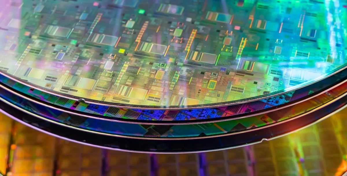

The global semiconductor landscape is currently undergoing a period of intense transformation, characterized by aggressive national industrial policies, rapid technological breakthroughs in AI-integrated architectures, and a persistent push toward supply chain diversification. As recent industry developments demonstrate, the sector is balancing the immediate pressures of market demand with long-term capital investments that will dictate the future of computing, automotive electronics, and artificial intelligence for the coming decade.
The Geopolitics of Silicon: National Strategies and Trade Shifts
The semiconductor industry has moved from a primarily market-driven ecosystem to one deeply embedded in national security and economic sovereignty. Recent data confirms that nations are moving beyond simple subsidies, focusing instead on building comprehensive, self-sustaining regional ecosystems.
India’s announcement of a $13.4 billion "Semicon 2.0" program underscores this trend, aiming to position the nation as a primary hub for semiconductor manufacturing, assembly, testing, and packaging (ATP). This follows the momentum established by the United States’ CHIPS and Science Act and the European Union’s European Chips Act. These policy frameworks are not merely funding mechanisms; they are designed to shift the geographic concentration of wafer fabrication—which currently remains heavily skewed toward East Asia—to a more distributed global footprint.
Simultaneously, the regulatory environment is tightening. Export controls, particularly regarding deep ultraviolet (DUV) lithography equipment and advanced chipsets, have become a permanent fixture of international trade relations. China’s ongoing efforts to enhance its domestic immersion DUV capabilities represent a strategic counter-response to these restrictions, creating a bifurcated market that threatens to decouple technology standards between East and West.
Technological Frontiers: From 2D Materials to Photonic Computing
Technological advancement remains the lifeblood of the semiconductor industry, with research and development (R&D) efforts increasingly focused on overcoming the physical limits of traditional silicon-based CMOS architecture.
A critical development is the emergence of 2D Tunnel Field-Effect Transistors (TFETs) and the exploration of molybdenum disulfide (MoS2) nanotubes. These materials offer the potential for lower power consumption and higher performance at sub-1nm scales, addressing the "AI burnout" associated with the massive energy requirements of large language model (LLM) training.
Furthermore, the industry is witnessing a transition toward heterogeneous integration. The movement toward heterogeneous High Bandwidth Memory (HBM) and 300mm silicon photonics represents a paradigm shift. By integrating optical interconnects directly onto the silicon wafer, engineers are effectively solving the bottleneck of data movement, which has historically hindered the scaling of AI compute clusters. In-memory photonic computing, which performs calculations directly within the memory array, is similarly gaining traction as a method to reduce the latency inherent in the von Neumann architecture.
The AI Integration Imperative
Artificial intelligence is no longer a peripheral application; it is the primary driver of semiconductor design. The industry is responding with a massive pivot toward specialized hardware.
Recent corporate activities, including significant investments in AI power management funding and the development of edge AI developer tools, highlight the dual-track nature of this evolution. Companies are simultaneously scaling up high-performance data center chips and refining edge AI capabilities to allow for real-time processing in autonomous vehicles and robotics.
However, this rapid scaling brings structural challenges. The industry is grappling with "AI pressure points"—the convergence of high thermal design power (TDP), the requirement for massive memory bandwidth, and the need for advanced packaging technologies to keep these complex chips operational. The push toward safe AI in Software-Defined Vehicles (SDVs) adds an additional layer of complexity, as hardware must now meet rigorous functional safety standards while delivering the computational throughput required for Level 4 and Level 5 autonomous driving.
Market Dynamics: Consolidation and Supply Chain Resilience
The financial side of the industry remains volatile. Recent merger and acquisition (M&A) activity, such as Onsemi’s pursuit of Synaptics, signals a broader trend of vertical integration. As semiconductor firms attempt to capture more value across the design-to-manufacturing spectrum, consolidation is becoming an attractive strategy to achieve the economies of scale necessary for R&D.
Supply chain stability is a lingering concern. While DRAM shortages and general chip scarcities have eased from their pandemic-era peaks, the focus has shifted to "strategic IC supply" mapping. McKinsey and other analytical firms have emphasized that the vulnerability of the industry lies in the upstream supply chain—specifically in the concentration of raw materials and specialized chemicals. Efforts like the $75 million allocation toward recycling rare earth materials are direct attempts to mitigate these upstream risks and promote a circular economy within the semiconductor industry.
Chronology of Key Industry Milestones (Q3-Q4)
- Policy Initiatives: The introduction of India’s Semicon 2.0 policy marks a significant shift in the global foundry landscape, aiming to attract major global players through tiered incentive structures.
- Infrastructure Expansion: Continued investment in Dresden’s power semiconductor hub and expansion efforts by Intel and UMC reflect a concerted effort to increase mature-node capacity, which remains vital for automotive and industrial sectors.
- R&D Milestones: IBM’s announcement regarding 7-angstrom chip technology with 40% improvements in SRAM area efficiency demonstrates that Moore’s Law is being extended through architectural ingenuity rather than just lithographic shrinking.
- Safety and Standards: The formation of AI security alliances and the development of new credentialing programs for PCB design reflect an industry-wide recognition that security and human capital are as important as hardware specifications.
Analysis: The Implications of the "New Normal"
The current trajectory of the semiconductor industry suggests three long-term implications for the global economy.
First, the cost of innovation is rising. As the industry moves toward 1nm processes and advanced packaging (such as 3D heterogeneous integration), the capital expenditure (CapEx) required for a single leading-edge fab has surpassed $20 billion. This cost floor effectively limits the number of players capable of competing at the highest tier, likely leading to further market concentration among a handful of global giants.
Second, the decoupling of the supply chain is likely to increase inflationary pressure on electronics. While domestic manufacturing provides security, it often lacks the cost-efficiency of the globalized, highly optimized supply chains that defined the last thirty years. Consumers and businesses should anticipate a permanent shift in the pricing structure of compute-heavy devices.
Third, the talent gap remains the most significant, yet least discussed, constraint. As evidenced by the proliferation of new credentialing and training programs, the industry is facing a severe shortage of engineers specialized in advanced packaging, photonic integration, and AI-optimized architecture. Bridging this gap will require sustained collaboration between academic institutions, private industry, and government entities over the next decade.
Official and Industry Responses
Industry leaders have largely adopted a cautious yet optimistic outlook. The Semiconductor Industry Association (SIA) has consistently advocated for the continued implementation of the CHIPS Act, arguing that long-term certainty is essential for private sector investment. In contrast, foundry executives have expressed concerns regarding the regulatory "patchwork" that global firms must navigate, noting that compliance with disparate national standards adds significant operational overhead.
Market analysts, while acknowledging the cyclical nature of the chip business, maintain that the "AI supercycle" is fundamentally different from previous demand spikes. The structural requirement for high-performance compute in almost every industrial sector—from manufacturing robotics to precision agriculture—suggests that the current investment cycle is grounded in long-term demand rather than temporary inventory accumulation.
Conclusion
The semiconductor industry stands at a crossroads. While the immediate focus remains on navigating geopolitical tensions and scaling AI-centric hardware, the underlying trend is toward a more resilient, localized, and technologically diverse architecture. Whether through the development of photonic interconnects, the adoption of 2D materials, or the implementation of circular supply chains, the industry is demonstrating remarkable adaptability.
As we look toward the next fiscal year, the focus will likely remain on the execution of these ambitious infrastructure projects and the stabilization of the supply chain in the face of ongoing global uncertainty. The semiconductor sector is no longer just a component supplier; it has become the foundational infrastructure of the modern state, and its trajectory will remain the most critical indicator of global technological progress for the foreseeable future.
