
The global electronic design automation (EDA) and semiconductor intellectual property (IP) sectors reached a significant financial milestone in the fourth quarter of 2025, recording total revenues of $5.466 billion. According to the latest Electronic Design Market Data (EDMD) report released by SEMI, this represents a 10.3% increase over the $4.955 billion reported during the same period in 2024. This performance marks a continuation of a multi-year trend of double-digit growth, underscoring the indispensable role of design tools and pre-verified functional blocks in the increasingly complex semiconductor manufacturing ecosystem. However, beneath the aggregate growth lies a more complex narrative of diverging performance across different product categories and geographic regions, particularly regarding the fluctuating fortunes of the IP market in China and the cooling of the physical design segment.
Core Financial Performance and Segment Breakdown
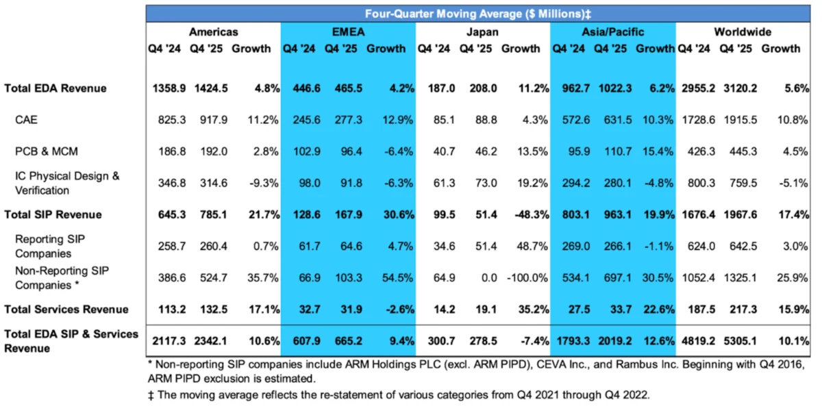
The fourth quarter of 2025 saw robust performance in several key categories, though the growth was not uniform across the board. Computer-Aided Engineering (CAE), which remains the largest single category within the EDA landscape, rose by 9.4% to reach $2.083 billion. This compares to $1.761 billion in the fourth quarter of 2024. CAE tools are foundational to the design process, encompassing synthesis, simulation, and verification—tasks that have become exponentially more compute-intensive as the industry moves toward 3nm and 2nm process nodes.

The semiconductor IP segment, which involves the licensing of pre-designed logic, memory, and interface blocks, provided the most striking data points in the report. The "non-reporting" IP companies—a category notably dominated by industry giant Arm—saw a massive surge of 24.7%, bringing in $1.413 billion compared to $1.134 billion in the previous year’s final quarter. In contrast, "reporting" IP companies—those that contribute direct data to the SEMI report—showed a more modest growth rate of 6.8%.
Other sectors showed varied results. The Printed Circuit Board (PCB) and Multi-Chip Module (MCM) segment grew slightly by 1.8%, reaching $484.6 million. This slow growth suggests a period of consolidation or perhaps a transition phase as designers shift toward advanced packaging technologies that blur the lines between traditional PCB design and semiconductor backend processes. Meanwhile, the services revenue category experienced a significant jump of 19.6%, totaling $233.9 million. This spike reflects an increasing reliance on external expertise as chip design firms grapple with the complexities of heterogeneous integration and AI-driven design methodologies.
A Nuanced Growth Picture: The "Arm" Effect and Regional Disparities
Walden Rhines, the executive sponsor of the SEMI Electronic Design Market Data Report and a veteran of the semiconductor industry, noted that the Q4 numbers suggest a "diversity of where [growth] came from." While the overall industry health appears strong, Rhines pointed to specific areas of concern, particularly within the IP business.

The divergence between reporting and non-reporting IP companies is one of the most significant trends highlighted in the Q4 data. While the total IP market grew by 18% on a worldwide basis, the reporting companies only managed a 6.8% increase. Over a broader four-quarter moving average, the disparity is even more pronounced: reporting companies have grown by only 3%, whereas non-reporting companies have surged by 25% to 26%. This suggests that a small number of dominant players, likely those specializing in high-demand processor architectures for data centers and AI, are capturing the lion’s share of the market’s expansion.
Geography also played a major role in the quarter’s results. The IP business in China was characterized as "very weak" during this period. This downturn is attributed to a combination of factors, including tightening trade restrictions on high-end design technologies and a localized shift in the Chinese semiconductor strategy. As Chinese firms face hurdles in accessing certain Western IP, there is an ongoing, albeit difficult, transition toward domestic alternatives or open-source architectures like RISC-V, which may not yet be reflected in the traditional reporting revenue streams.
Chronology of Market Evolution: From 1996 to 2025
The growth observed in 2025 is part of a long-term trajectory that began in the mid-1990s. In 1996, the combined EDA and SIP market was a fraction of its current size, focused largely on basic logic synthesis and physical layout tools. Throughout the early 2000s, the market matured as the industry moved from "system-on-a-board" to "system-on-a-chip" (SoC) architectures, necessitating more sophisticated IP blocks.

By the mid-2010s, the emergence of mobile computing and the initial waves of cloud infrastructure demand began to drive the double-digit growth cycles that have now become the standard. The period between 2020 and 2025 has been particularly transformative, fueled by the "AI Gold Rush" and the necessity of specialized silicon. The fourth quarter of 2025 represents the latest peak in this nearly 30-year climb, though the current volatility in the physical design segment suggests the industry may be entering a new phase of technical challenges.
Physical Design and Verification: A Surprising Decline
One of the most notable "weak areas" identified in the report was physical design and verification. This segment saw a year-over-year revenue decline of 2.6%, falling to $797.9 million. This contraction is counter-intuitive to some, given that physical design—the process of turning a logical circuit into a physical layout on silicon—is generally considered more difficult at advanced nodes.
Industry analysts suggest several reasons for this dip. First, quarterly fluctuations can be influenced by the timing of major software license renewals. Second, there is the "front-end/back-end" lag. Issues at the back end of the manufacturing flow—such as supply shortages in critical materials or bottlenecks in advanced packaging facilities—can cause companies to delay the start of new designs at the front end. Furthermore, the increasing use of AI-enhanced EDA tools may be changing the pricing models or the efficiency of the design process itself, leading to a temporary plateau in revenue as the industry adjusts to higher productivity per license.

Broader Implications for the Semiconductor Ecosystem
The data from Q4 2025 carries significant implications for the broader technology sector. The strength in CAE and services suggests that while companies are still investing heavily in the "brains" of the chip—the architecture and the logic—they are increasingly seeking help to navigate the physical realities of modern manufacturing.
- The AI Influence: The massive growth in non-reporting IP companies (principally Arm) points to the continued dominance of high-performance compute architectures. As AI moves from the data center to the edge, the demand for high-efficiency, pre-verified processor IP is expected to remain the primary driver of market expansion.
- Geopolitical Realignments: The weakness in the Chinese IP market is a signal of the "de-coupling" of the global semiconductor supply chain. While this creates short-term revenue headwinds for Western IP providers, it is accelerating the development of independent ecosystems, which may lead to more fragmented standards in the future.
- The Complexity Gap: The growth in services revenue (19.6%) highlights a growing "complexity gap." Even large semiconductor firms are finding it difficult to maintain all the necessary expertise in-house to handle 2.5D and 3D packaging, thermal management, and signal integrity at sub-5nm scales. This creates a lucrative niche for specialized EDA service providers and consultants.
- Supply Chain Interdependence: As Walden Rhines noted, the EDA and IP markets do not exist in a vacuum. Trade restrictions, memory supply shortages, and even geopolitical conflicts affecting raw materials can disrupt the flow of new design starts. The Q4 data serves as a reminder that the "front end" of the industry is deeply tied to the "back end" realities of the global supply chain.
Conclusion and Future Outlook
As the industry moves into 2026, the EDA and semiconductor IP sectors remain on a solid, albeit more complex, footing. The total revenue of $5.466 billion for Q4 2025 is a testament to the essential nature of these technologies. However, the stagnation in physical design and the geographic shifts in the IP market suggest that the "easy" growth of the past few years may be evolving into a more competitive and specialized landscape.
Stakeholders will be watching closely to see if the reporting IP companies can close the growth gap with non-reporting giants, and whether the decline in physical design is a temporary blip or a sign of a fundamental shift in how chips are designed. For now, the double-digit growth streak remains intact, fueled by the global hunger for increasingly sophisticated silicon solutions. The SEMI EDMD report provides a vital snapshot of an industry that is simultaneously the foundation of modern technology and a mirror of its most pressing geopolitical and technical challenges.
