
The global semiconductor industry is currently navigating a fundamental transition in how advanced microchips are assembled, moving away from the traditional circular 300mm silicon wafer toward large, rectangular panel-level processing. While the concept of panel-level packaging (PLP) has existed for over a decade, it has historically remained a niche solution, often retreating into research labs when the mechanical complexities of handling large rectangular formats outweighed the immediate financial benefits. However, the explosive growth of Artificial Intelligence (AI) accelerators and High-Performance Computing (HPC) modules has fundamentally altered the industry’s cost-benefit analysis. As chip architectures grow physically larger and more complex, the limitations of wafer-level economics are reaching a breaking point, forcing a shift toward the superior area efficiency of panels.
The Scaling Crisis of Circular Wafers
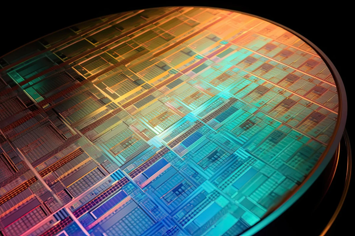
For decades, the 300mm silicon wafer has been the gold standard for semiconductor manufacturing. However, as the industry enters the era of "system-in-package" (SiP) and heterogeneous integration, the physical dimensions of the final package are expanding. Modern AI accelerators often incorporate multiple logic dies and several stacks of High Bandwidth Memory (HBM), creating a footprint that consumes a significant portion of a standard wafer.
The economic strain stems from a simple geometric reality: a circle is an inefficient container for large squares. As the area of an individual package increases, the number of units that can fit on a 300mm wafer drops precipitously. Furthermore, the "edge loss"—the unusable space around the perimeter of the wafer—increases as packages grow. When a single processing run yields only a handful of viable units, the fixed costs of lithography, deposition, and etching are spread across too few sellable products.
Industry leaders now argue that packaging has become the primary bottleneck for continued scaling. Sesha Varadarajan, senior vice president of the global products group at Lam Research, noted in a recent keynote that packaging is now as vital to scaling as transistor density. He emphasized that advanced packaging is no longer just about increasing Input/Output (I/O) density but is becoming the foundational architecture for incorporating silicon photonics and other novel device types into a single, cohesive module.
Historical Context: From Standard Fan-Out to HPC Necessity
The industry is currently witnessing what experts call the "second wave" of panel fan-out technology. The first wave, which emerged several years ago, focused primarily on standard fan-out approaches—relatively simple packages produced on large panels to reduce costs for consumer electronics. That wave saw limited adoption because the infrastructure for handling large panels was not yet mature, and the cost savings for small chips did not always justify the capital expenditure for new equipment.
The current second wave is different because it is driven by necessity rather than just incremental cost reduction. Amy Lujan, president at SavanSys, recently highlighted that the demands of HPC and AI chips are forcing a re-evaluation of advanced process flows. Current interest is centering on intermediate panel formats, such as the 310mm x 310mm range. These formats offer a meaningful increase in surface area over 300mm wafers without requiring the massive, and often risky, leap to the largest proposed industrial panels (600mm x 600mm). This step-wise progression allows manufacturers to improve units-per-run economics while managing the mechanical stresses inherent in rectangular substrates.
The Material Frontier: Transitioning to Glass Substrates
Central to the discussion of panel-level packaging is the emergence of glass as a primary substrate material. Traditionally, organic substrates have been used, but they suffer from dimensional instability, significant warpage at large sizes, and dielectric loss at high frequencies. Glass offers a compelling alternative due to its extreme flatness, smooth surface for fine-pitch routing, and a coefficient of thermal expansion (CTE) that can be engineered to match silicon.
However, the transition to glass introduces a significant engineering trade-off: brittleness. Unlike silicon or organic polymers, glass does not deform gracefully under stress; it cracks. Jonas Discher, head of sales for wafer-level and advanced packaging at Plan Optik AG, warned that micro-cracks introduced during the initial raw material preparation can act as stress concentration points. These defects may remain invisible through early processing steps only to cause catastrophic failure during thermal cycling or mechanical handling later in the flow. As panel sizes increase, the cumulative risk of these failures grows, making surface integrity a primary concern for high-volume manufacturing.
Overcoming the "TGV" Failure Mechanism
One of the most complex technical hurdles in panel-level glass processing involves Through-Glass Vias (TGVs). These are the vertical electrical connections that allow signals to pass through the substrate. Because copper (used for the vias) and glass have different thermal expansion rates, heating and cooling cycles create intense mechanical tension.

Poulomi Mukherjee, a process integration engineer at Applied Materials, explained that during heating, copper expands more than the surrounding glass, creating a stress concentration point. During the subsequent cooling phase, the copper pulls on the glass, initiating circumferential cracks. To solve this, researchers have had to move beyond simple material substitution toward complex co-engineering.
Applied Materials has found that an optimized solution requires a specific liner material—one with both a low CTE and a low modulus. The low CTE compensates for the mismatch between the copper and glass, while the low modulus allows the material to deform slightly, absorbing the strain energy that would otherwise shatter the glass. Such innovations illustrate that panel-level packaging is as much a materials science challenge as it is a mechanical one.
Warpage and the Precision of Temporary Bonding
At the panel scale, "warpage"—the tendency of a substrate to bow or curl—becomes a systemic threat. This is not merely an end-of-line defect but a cumulative result of every process step, from the curing of polymers to the density of copper layers.
Temporary bonding materials, which hold the substrate in place during thinning and processing, are often the unsung culprits of warpage. Hamed Gholami Derami of Brewer Science noted that if a bonding layer is not perfectly uniform across a 310mm panel, subsequent grinding steps will result in uneven die thickness. This variation then ripples through the assembly process, causing alignment errors in interconnects and ultimately destroying the yield. Consequently, the industry is calling for a new generation of temporary bonding materials specifically designed for the thermal and mechanical demands of large-rectangular formats.
The Cleanroom Paradox: Hybrid Bonding at the OSAT Level
The push for panel-level packaging is also colliding with the rise of hybrid bonding—a technique that allows for ultra-high-density interconnects between chiplets. Hybrid bonding was pioneered in semiconductor foundries, where "Class 1" cleanroom standards are the norm. However, as this technology migrates to Outsourced Semiconductor Assembly and Test (OSAT) providers to support panel-based packages, a cleanliness gap has emerged.
Mike Kelly, vice president at Amkor, emphasized that particle contamination is a "death knell" for hybrid bonding. Even a single nano-sized particle can prevent a bond from forming, potentially ruining an entire large-format panel. Because OSAT facilities are traditionally not built to foundry-level cleanliness standards, equipment manufacturers are now developing "cluster tools." These machines create localized ultra-clean environments within the tool itself, allowing OSATs to perform high-precision bonding without the multi-billion-dollar cost of upgrading an entire facility’s air filtration system.
Digital Twins and the Simulation of Unprecedented Scales
Perhaps the most daunting aspect of the shift to panels is that engineers are often designing processes for structures that do not yet exist at scale. The physical behavior of a 100mm x 150mm package spanning dozens of lithographic reticle fields is difficult to predict using standard wafer-based models.
Sutirtha Kabir, executive director of R&D at Synopsys, pointed out that modern AI package designs are moving toward using several dozen reticles. A design of this scale might include 30 or more embedded silicon bridges, each requiring precision alignment. Modeling how such a massive, multi-component structure will react to 20 or more sequential process steps is a computational challenge of the highest order. The industry currently lacks a comprehensive database of how different glass formulations behave under mass production, and manufacturers are often hesitant to share the proprietary data needed to build more accurate simulation tools.
Conclusion: A Fundamental Re-engineering of the Backend
The transition from 300mm wafers to large-scale panels represents a "coming of age" for semiconductor packaging. It is no longer a secondary concern that follows chip fabrication; it has become the primary theater for innovation and cost management in the AI era.
The economic drivers are undeniable: as AI accelerators grow in size, the circular wafer format becomes unsustainable. However, the path to successful panel-level processing is fraught with engineering obstacles. Success will require a holistic integration of materials science, new equipment architectures, and advanced simulation. The companies that successfully navigate these "hard" engineering problems—solving for glass brittleness, TGV stress, and cleanroom contamination—will define the next decade of the global semiconductor supply chain. The work ahead is not simply about making things bigger; it is about re-engineering the very foundation of how the world’s most powerful computers are built.
