
As the global demand for artificial intelligence (AI) and high-performance computing (HPC) continues to surge, the physical limitations of traditional copper-based data transmission have become a primary bottleneck for hardware architects. While optical fiber has long been the standard for long-distance telecommunications due to its superior speed and efficiency, the industry is now witnessing a concerted effort to miniaturize these optical components for use over much shorter distances. The goal is to integrate photonics directly into the racks, boards, and eventually the silicon packages that house the world’s most powerful processors. This shift is not merely a matter of incremental improvement; it is a fundamental necessity driven by the unique and voracious data requirements of modern Large Language Models (LLMs) and the massive GPU clusters that train them.
The urgency of this transition was underscored last year when the semiconductor giant AMD acquired Enosemi, a specialized silicon photonics startup. This acquisition highlighted a growing consensus among industry leaders: the future of high-performance silicon is inextricably linked to the ability to move data using light rather than electricity. In a white paper published prior to the acquisition, Enosemi estimated that leading-edge high-performance Application-Specific Integrated Circuits (ASICs) currently expend as much as 50% of their total power budget simply on data movement. In an era where data center power consumption is under intense regulatory and environmental scrutiny, such inefficiency is increasingly untenable.
The Divergent Demands of AI Traffic
To understand why silicon photonics has moved to the forefront of the semiconductor roadmap, one must examine the specific nature of AI workloads. Traditional high-performance computing tasks often involve "North-South" traffic, where data moves between the end user and the data center. While an AI query, such as a prompt sent to a chatbot, may look like a conventional search query in terms of North-South volume, the internal operations required to generate a response are vastly different.
AI workloads rely heavily on "East-West" traffic—the movement of data between individual GPUs and across server racks within the data center. GPU clusters perform relatively straightforward mathematical operations, such as multiplication and addition, on massive data arrays. However, the sheer scale of these arrays means that the required bandwidth often limits the overall performance of the system. This "bandwidth wall" is compounded by the fact that moving these vast quantities of data over copper traces generates significant heat and consumes a disproportionate amount of electricity. As GPU clusters scale from hundreds to tens of thousands of units, the energy cost of electrical interconnects threatens to eclipse the energy used for actual computation.
Metrics of Interconnect Efficiency
Mike Hogan, the Chief Business Officer at GlobalFoundries, has identified four critical metrics that define the efficiency and viability of any interconnect technology in the modern era: power efficiency, bandwidth density, latency, and cost-effectiveness. Currently, electrical interconnects are struggling to keep pace across these categories as distances increase.
At very short distances, the physical size of optical components has historically been a disadvantage, limiting the bandwidth density compared to tightly packed copper traces. However, as the industry moves toward more advanced manufacturing processes, the need to scale optical components alongside electronic circuits has become a primary engineering challenge. To capture the inherent energy savings of photonic interconnects, designers are currently evaluating three distinct integration concepts, each suited to different layers of the data center architecture.
The first and most mature concept is pluggable components. These are modular, relatively large devices that are easy to integrate into existing systems. However, their size necessitates longer electrical connections to the control circuitry, which introduces some signal degradation. Pluggables remain the preferred choice for connections between different boards or across the span of a data center.
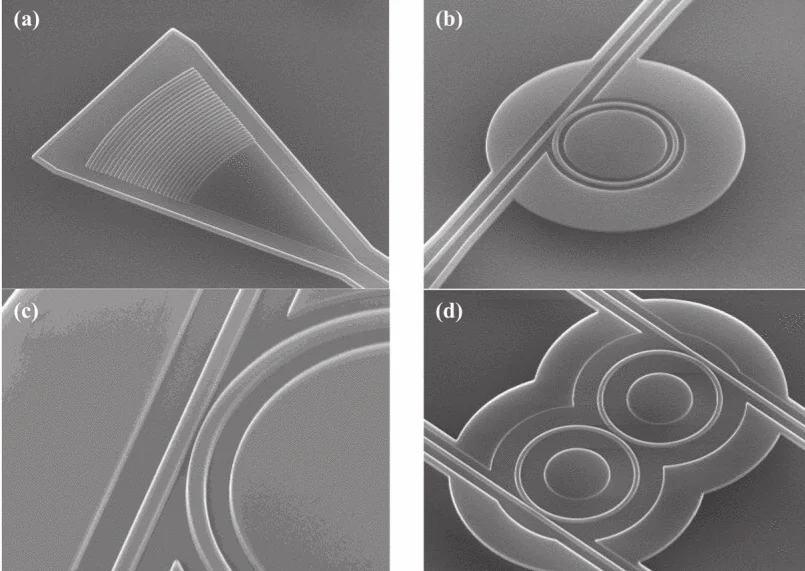
The second concept is Co-packaged Optics (CPO). As the name suggests, CPO involves the integration of discrete optical elements with electronic control circuits within a single package, typically using wire bonds for connectivity. This reduces the distance the electrical signal must travel, thereby improving efficiency.
The third and most advanced concept is Optical I/O (OIO) modules. These modules combine optical and electronic integrated circuits (ICs) into a unified device that effectively functions as a single unit. OIO represents the ultimate goal of silicon photonics, offering the highest bandwidth density and the lowest power consumption by bringing the optical interface as close to the processor core as possible.
The Essential Building Blocks of Silicon Photonics
The architecture of a photonic interconnect, regardless of its scale, relies on several fundamental building blocks. The process begins with a light source, typically an indium phosphide (InP) diode laser. Because lasers must operate under high currents and temperatures, they are often the most fragile component in the system. In pluggable systems, the ability to easily replace a failing laser is a significant advantage. However, for integrated OIO modules, ensuring the reliability of the laser—or developing "known good" laser testing protocols—is critical to the yield of the final package.
Once the laser provides a continuous beam of light, a modulator is required to "encode" data onto that beam by breaking it into a stream of bits. This component defines the transmission rate of the system. Recent research presented by Joris Van Campenhout of imec at the IEEE Electron Device Meeting suggests that materials like lithium niobate (LiNbO3) can achieve bandwidths exceeding 100 GHz with exceptional efficiency. The challenge, however, lies in the fact that lithium niobate has a large physical footprint and poses a contamination risk in conventional silicon fabrication environments.

To circumvent this, researchers in Singapore have successfully utilized microtransfer printing. This process uses a specialized stamp to pick and place patterned lithium niobate modulators from a growth wafer onto a silicon substrate. Other companies, such as NLM Photonics, are exploring organic materials, such as chromophore-doped glasses, which can be switched via adjacent silicon components to achieve high-speed modulation without the bulk of traditional crystals.
After the signal is modulated, it travels through a waveguide. Silicon itself serves as an excellent low-loss waveguide for the wavelengths of light typically used in data centers. Finally, the signal reaches a photodetector, where it is converted back into an electrical signal. Germanium is the material of choice for photodetectors due to its high sensitivity and compatibility with silicon processes.
Overcoming Manufacturing and Thermal Challenges
The path to full electrical-optical integration is fraught with mechanical and thermal hurdles. Heterogeneous integration—combining different materials and chiplets into a single package—is a complex task that requires new design rules. For instance, researchers at CEA-Leti have been working on embedding waveguides within silicon interposers. These interposers must facilitate optical paths to surface-mounted lasers while also utilizing through-silicon vias (TSVs) for electrical connectivity.
One of the most significant issues discovered during this research is the impact of mechanical stress. The physical pressure of the packaging process can cause optical distortions in the waveguides, leading to signal loss. Consequently, engineers must now use advanced modeling tools that account for both the electrical and optical effects of thermal and mechanical stress.
Thermal management is another critical factor. In many silicon photonic designs, small heaters are used to control the resonant frequency of microring modulators. While effective, these heaters can be energy-intensive. CEA-Leti has demonstrated that by thermally isolating these components, significant energy savings can be achieved, further improving the "picojoules per bit" metric that is so vital to data center operators.
Furthermore, the cost of manufacturing remains a barrier. Epitaxial growth of germanium for photodetectors, for example, can account for nearly 40% of the total circuit cost because the layers must be significantly thicker than the silicon-germanium used in standard transistors. To address this, companies like NTT are experimenting with bonding entire indium phosphide wafers to silicon wafers for in situ laser growth, a method that could potentially lower costs through economies of scale.
Chronology of Development and Industry Alignment
The evolution of silicon photonics has followed a clear timeline, moving from the periphery of the network to the heart of the chip. In the early 2000s, the technology was largely experimental, confined to university laboratories and niche telecommunications applications. By the mid-2010s, the rise of cloud computing led to the adoption of 100G and 400G pluggable optical transceivers, which became the backbone of the modern data center.
The current era, beginning around 2022, is defined by the "AI Boom." The massive scale-out of NVIDIA, AMD, and Intel hardware has shifted the focus from rack-to-rack communication to chip-to-chip communication. The 2023 acquisition of Enosemi by AMD serves as a pivotal marker in this chronology, signaling that the world’s largest chipmakers are no longer treating photonics as a secondary technology, but as a core competency.
Industry leaders agree that the status quo is unsustainable. As Mike Hogan noted, there is now a "strong alignment" across compute vendors, network leaders, and silicon suppliers. The industry is moving toward a future where the distinction between an electronic chip and an optical module begins to blur.
Implications for the Global Technology Landscape
The successful integration of silicon photonics will have profound implications for the global technology landscape. Beyond the immediate performance gains for AI training, the reduction in power consumption is a critical factor for the sustainability of the digital economy. If optical I/O can successfully reduce the energy required for data movement by 50%, it would represent one of the most significant efficiency gains in the history of computing.
Furthermore, this shift will likely trigger a realignment of the semiconductor supply chain. Fabs that have traditionally focused solely on CMOS (Complementary Metal-Oxide-Semiconductor) processes must now develop expertise in handling exotic materials like Indium Phosphide and Lithium Niobate. The ability to manufacture these hybrid "electro-optical" chips at scale will become a key competitive advantage for foundries and integrated device manufacturers alike.
While substantial work remains in refining manufacturing yields and perfecting thermal management, the goal is clear. To sustain the growth of artificial intelligence and manage the astronomical data demands of the future, the industry must stop relying on the movement of electrons over copper and start embracing the speed of light. The transition to silicon photonics is no longer a matter of "if," but "how fast."
