
The semiconductor industry is currently navigating a period of unprecedented architectural complexity, driven by the demand for high-performance computing, artificial intelligence (AI), and autonomous systems. As chips transition from simple integrated circuits to massive Systems-on-Chip (SoCs) featuring billions of transistors and hundreds of heterogeneous cores, the traditional methods of ensuring these designs work as intended are reaching their breaking point. In this environment, achieving a deterministic "yes or no" answer regarding a design’s correctness has become a monumental task. The reliance on simulation—a method that tests a design against a set of predetermined stimuli—is no longer sufficient to guarantee the absence of bugs in the vast state space of modern silicon.
Ashish Darbari, CEO of Axiomise, recently highlighted the critical shift toward formal verification (FV) as a primary driver for reducing time-to-sign-off. Unlike simulation, which can only prove the presence of bugs, formal verification uses mathematical proofs to verify that a design meets its specification under all possible conditions. However, the complexity of modern designs means that even formal tools can struggle with "state-space explosion," where the number of possible configurations exceeds the tool’s computational capacity. To combat this, the industry is increasingly looking toward the identification and application of common patterns in design and verification to streamline the process and ensure higher coverage.
The Evolution of Verification Complexity
The history of semiconductor verification is a chronicle of the industry’s attempt to keep pace with Moore’s Law. In the 1980s and early 1990s, verification was largely a manual process, relying on directed tests where engineers wrote specific sequences of inputs to check basic functionality. This paradigm shifted in the late 1990s and early 2000s with the advent of constrained-random verification (CRV) and the Universal Verification Methodology (UVM). These methods allowed for the automated generation of test cases, but they still relied on the probability of hitting a bug rather than the certainty of its absence.
The pivotal moment for formal verification occurred in 1994 with the infamous Intel Pentium FDIV bug, which cost the company approximately $475 million. This event underscored the limitations of simulation and spurred the development of formal methods in the mainstream. Over the last decade, the focus has shifted again. We are no longer just verifying that a chip "works"; we are verifying that it is safe from physical failure and secure against malicious intent. As Darbari points out, the interaction between functional logic, safety mechanisms, and security protocols creates a multidimensional verification problem that is nearly impossible to solve through simulation alone.
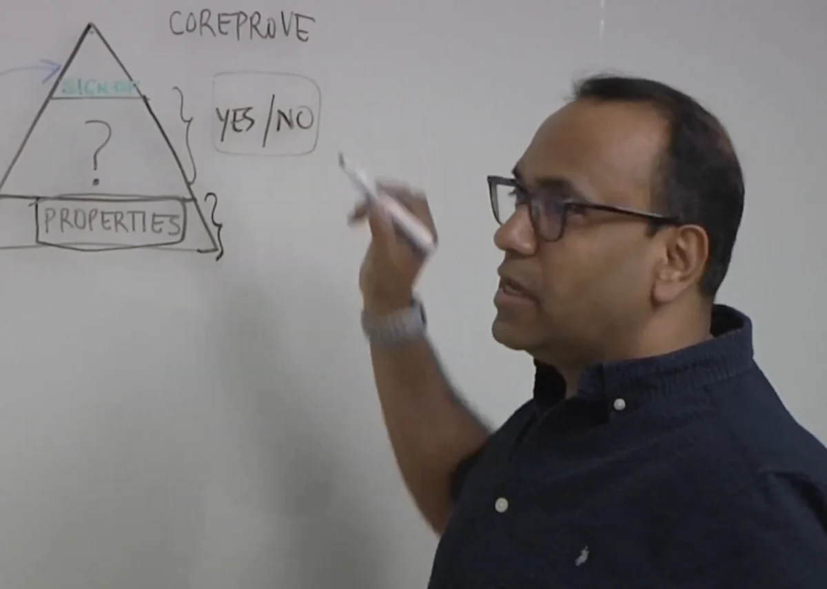
Deciphering the Deterministic Challenge
The primary goal of verification sign-off is to reach a point of "deterministic certainty," where the engineering team can confidently state that the design is ready for tape-out. In a simulation-centric world, this certainty is measured in "coverage," a metric that tracks which parts of the code have been exercised. However, high coverage in simulation does not equate to the absence of bugs; it merely means the tested scenarios didn’t fail.
Formal verification offers a deterministic alternative. By using mathematical solvers to explore every possible input combination over time, formal tools can provide a definitive proof of correctness. The challenge, however, is that as designs grow, the "proof" becomes computationally expensive. This is where the concept of "patterns" becomes essential. By identifying recurring structures in hardware design—such as standard bus protocols (AXI, AHB), memory controllers, and interrupt handlers—verification engineers can apply pre-validated formal properties. This "pattern-based" approach allows teams to reach sign-off faster by focusing human expertise on the unique, custom logic of the chip while automating the verification of standard components.

The Role of Patterns in Formal Verification
Patterns in formal verification serve as a blueprint for how specific types of hardware should behave. Ashish Darbari emphasizes that these patterns are not just about the code itself, but about the intent behind the design. For instance, in a multi-core processor, the patterns of cache coherency are well-understood. Instead of reinventing the verification strategy for every new chip, engineers can use established formal models of coherency protocols to check for deadlocks and data corruption.
Beyond standard protocols, patterns also emerge in how bugs manifest. Common issues such as "off-by-one" errors in counters, race conditions in clock-domain crossings, and priority inversion in schedulers follow predictable mathematical signatures. Axiomise and other leaders in the formal space are advocating for the use of "Formal Property Verification" (FPV) templates that capture these signatures. By applying these templates, engineers can find deep, corner-case bugs in hours that might have taken weeks to find—or might have been missed entirely—using simulation.
Safety and Security: The New Frontiers
As the industry moves toward AI-driven automotive systems and sensitive edge computing, the stakes for verification have moved beyond mere functionality. Safety standards like ISO 26262 require rigorous proof that a chip will behave predictably even in the presence of hardware faults. Similarly, security requirements demand that sensitive data cannot be leaked through side-channels or unauthorized access points.
Formal verification is uniquely suited for these tasks. In safety verification, formal tools are used for "fault injection" analysis, where the tool mathematically proves whether a design can recover from a bit-flip caused by cosmic radiation. In security, formal methods can verify "non-interference" properties, ensuring that a low-security process cannot observe the activity of a high-security process. Darbari notes that identifying patterns in how safety and security mechanisms interact is the next great hurdle. When a security protocol blocks a certain action, does it inadvertently create a safety hazard by causing a system timeout? Formal verification provides the mathematical framework to analyze these cross-functional interactions.
AI-Driven Design and the Verification Paradox
The rise of AI presents a paradox for the semiconductor industry. On one hand, AI is the primary driver for the current boom in chip design, with companies racing to build more powerful Neural Processing Units (NPUs). On the other hand, the non-linear and highly parallel nature of AI architectures makes them incredibly difficult to verify.
Interestingly, AI is also being used to improve the verification process itself. EDA (Electronic Design Automation) tools are now incorporating machine learning to predict which parts of a design are most likely to contain bugs and to optimize the formal solver’s path through the state space. This creates a feedback loop: AI helps build the chips, and the chips, in turn, provide the horsepower for the AI that verifies the next generation of silicon. Darbari suggests that the integration of AI with formal patterns will be the key to managing the "sign-off" of future 2nm and 3nm designs.
Supporting Data and Industry Metrics
The shift toward formal verification is supported by sobering economic data. According to industry studies by organizations like Wilson Research Group and Mentor (a Siemens Business), verification now accounts for approximately 60% to 70% of the total design cycle for complex SoCs. Furthermore, the cost of a "respin"—the need to manufacture a chip again due to a discovered bug—can exceed $5 million for a 7nm design, rising exponentially as the industry moves toward 3nm and 2nm nodes.

| Metric | Simulation-Based Approach | Formal-Pattern Approach |
|---|---|---|
| Coverage Type | Probabilistic (hit or miss) | Deterministic (mathematical proof) |
| Bug Discovery Time | Late in the cycle (post-integration) | Early in the cycle (shift-left) |
| State-Space Coverage | Limited by test-bench stimuli | Exhaustive (within constraints) |
| Sign-off Confidence | High (but with residual risk) | Absolute (for verified properties) |
| Engineer Effort | High (writing/maintaining tests) | Moderate (defining properties/patterns) |
Data from Axiomise suggests that by leveraging formal patterns, companies can achieve a "shift-left" in their timeline, identifying 80% of critical bugs before the first simulation environment is even fully functional. This reduction in the "verification gap"—the distance between what we can design and what we can verify—is the primary driver for the adoption of formal methods.
Official Responses and Industry Outlook
The push for formal-driven sign-off is gaining traction among major semiconductor players. Companies like Intel, NVIDIA, and ARM have long maintained dedicated formal verification teams, but the practice is now trickling down to smaller startups, particularly those in the RISC-V ecosystem. The open-source nature of RISC-V allows for a community-driven set of formal patterns, which Darbari and Axiomise have been instrumental in developing.
In statements regarding the future of the industry, leaders at major EDA vendors such as Cadence and Synopsys have echoed the sentiment that "verification is the bottleneck of innovation." They emphasize that the future of EDA lies in "Intelligent System Design," where formal verification is not an isolated step but an integrated part of the entire lifecycle, from architectural specification to post-silicon validation.
Broader Impact and Implications
The implications of faster, more reliable verification sign-off extend far beyond the balance sheets of semiconductor companies. In the automotive sector, the ability to formally prove the safety of an autonomous driving chip is a prerequisite for public trust and regulatory approval. In the realm of national security, the ability to verify that a chip is free of "hardware Trojans" or backdoors is a matter of geopolitical importance.
Furthermore, the democratization of formal verification through the use of patterns and automated tools is lowering the barrier to entry for custom silicon. As it becomes easier and faster to verify complex designs, we can expect a surge in domain-specific architectures—chips designed for very specific tasks like genomics, climate modeling, or real-time language translation.
In conclusion, the move toward pattern-based formal verification represents a fundamental shift in how hardware is validated. By moving away from the "brute force" method of simulation and toward the "intelligent application" of mathematical proofs, the industry is finding a path through the complexity of the AI era. As Ashish Darbari and other experts suggest, the goal is no longer just to find bugs, but to build an airtight case for a design’s correctness, ensuring that the chips powering our world are as reliable as the laws of mathematics themselves.
