
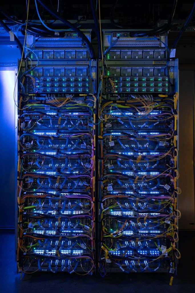
Google has announced a significant evolution in its Tensor Processing Unit (TPU) strategy, introducing two distinct chips for the eighth generation: the TPU 8t, optimized for training, and the TPU 8i, tailored for inference. This move, unveiled at the recent Google Cloud Next event, signals a departure from the company’s decade-long approach of delivering a single, albeit sometimes varied, chip architecture for both pre-training and inference workloads. The rationale behind this bifurcation lies in the rapidly diverging demands of modern AI, particularly the rise of agentic workloads, which Google argues necessitates specialized hardware for peak price-performance.
For much of its ten-year history, Google’s TPU lineage has been characterized by a unified architectural design. Each generation, while potentially offering variations in its Stock Keeping Units (SKUs), was built upon a singular foundation intended to handle the computationally intensive task of pre-training cutting-edge models and the subsequent, often high-volume, task of running inference on them. However, the increasing complexity and unique requirements of contemporary AI applications, especially those involving agentic systems and intricate reasoning processes, have rendered this monolithic approach suboptimal. Google’s assertion is that the pursuit of optimal price-performance at the frontier of AI acceleration can no longer be achieved by a single, generalized chip.
Two Chips, One Family: A Specialized Approach to AI Acceleration
The TPU 8t retains key elements of its predecessors, including the robust 3D torus interconnect. This network topology arranges chips in a three-dimensional grid where each dimension wraps around, providing each chip direct communication links to its six nearest neighbors. This architecture is crucial for efficient data distribution and communication in large-scale training clusters. Additionally, the TPU 8t continues to feature Google’s specialized SparseCores, designed to accelerate the irregular memory access patterns inherent in embedding lookups, a common operation in many machine learning models.
In contrast, the TPU 8i introduces a significant architectural overhaul, replacing the SparseCores with a novel on-die Collectives Acceleration Engine. Google claims this engine can reduce the latency of global synchronization operations by up to five times. These operations are critical for advanced inference techniques such as chain-of-thought decoding and the routing within Mixture-of-Experts (MoE) models, both of which are becoming increasingly prevalent in sophisticated AI systems. The network topology also undergoes a transformation, moving away from the 3D torus.
The TPU 8i adopts a new network layout inspired by the Dragonfly architecture, termed "Boardfly." This hierarchical topology prioritizes direct, high-speed connections. Within small groups of chips, all are fully interconnected. These groups are then linked to one another using direct optical long-haul cables, bypassing the need to route traffic through a traditional grid. While a torus excels at neighbor-to-neighbor communication, Dragonfly architectures are engineered for short communication paths between any two chips in a large system. Google reports that this new layout dramatically reduces the maximum hop count for a 1,024-chip pod from 16 to just 7.

Perhaps the most critical advancement in the TPU 8i is its design to address the "memory wall." The chip significantly increases on-chip Static Random-Access Memory (SRAM), tripling it to 384 MB. Furthermore, its High Bandwidth Memory (HBM) capacity is boosted to 288 GB. Google suggests this capacity is sufficient to hold the key-value (KV) cache for long-context reasoning models entirely within the chip’s silicon. In agentic workflows, every off-chip memory access introduces latency that directly impacts user-facing responses and compounds with each reasoning turn. Therefore, keeping the active working set on-chip is paramount for achieving responsive and efficient inference. This focus on memory capacity and bandwidth explains why the TPU 8i boasts higher per-chip bandwidth than the TPU 8t, a characteristic that might seem counterintuitive when considering training as typically the more compute-bound workload. However, agentic inference is increasingly becoming memory-bound.
The Strategic Rationale: Why Now?
The shift to specialized chips for training and inference is a departure from Google’s positioning just a year prior. At the launch of its seventh-generation TPU, codenamed "Ironwood" and still its flagship in general availability, Google marketed it as "the first Google TPU for the age of inference," emphasizing its capability for pre-training, training, and large-scale serving on the same silicon.
The fundamental demands of training and inference have always differed. However, the landscape of inference has undergone a dramatic transformation over the past year. Traditional inference, exemplified by early chatbot systems responding to a single prompt with a single output, represents one type of workload. In stark contrast, agentic inference involves a primary agent that decomposes a complex goal into subtasks, which are then dispatched to a fleet of specialized agents. These agents engage in long, iterative reasoning loops, placing significantly higher demands on KV cache size, all-to-all collective operations, and tail latency – metrics where the TPU 8i excels.
The evolution of AI models themselves also plays a crucial role. The increasing adoption of Mixture-of-Experts (MoE) architectures, which benefit immensely from high memory bandwidth, further bolsters the case for specialized inference hardware.
The training workload has not remained static either. Frontier models now necessitate clusters comprising hundreds of thousands of chips to achieve convergence within reasonable timelines. The TPU 8t superpod scales to 9,600 chips, and Google’s new Virgo data center fabric, coupled with its Pathways software, can logically stitch together more than a million TPU 8t chips into a single, massive training cluster. Google claims that the TPU 8t offers approximately 2.7 times better price-performance for training compared to Ironwood. For inference, the TPU 8i is projected to deliver 80 percent better price-performance. The ultimate validation of these claims will, of course, come from customer benchmarks.
A Divergent Path: Contrasting with AWS and Nvidia

Google’s strategic bifurcation of its TPU architecture stands in contrast to the approach taken by Amazon Web Services (AWS). At AWS re:Invent 2025, Amazon introduced Trainium3, explicitly stating its capacity to handle both training and inference. The company has effectively phased out its Inferentia line, signaling a belief that inference is increasingly mirroring training demands as models grow larger and reasoning chains extend. AWS’s perspective is that the gap between training-optimized and inference-optimized silicon is narrowing, not widening. Google’s eighth-generation TPUs represent a public bet against this thesis.
Nvidia occupies a different niche in this evolving landscape. The Vera Rubin NVL72 platform, which Google is reselling through its new A5X bare-metal instances, is a single-rack solution designed for both training and inference. On a per-chip basis, Nvidia’s Rubin GPU is considerably more powerful than either TPU 8 variant. For instance, it offers approximately 50 Petaflops of NVFP4 inference per GPU, compared to the TPU 8i’s 10.1 FP4 Petaflops per chip. However, when considering pod-level performance, the scales can invert. An NVL72 rack can reach close to 3.6 Exaflops of NVFP4 inference, while a TPU 8i pod, comprising 1,152 chips, can achieve 11.6 Exaflops of FP8 performance. This highlights differing philosophies: Nvidia focuses on fewer, more powerful chips interconnected via NVLink, whereas Google leverages many smaller chips orchestrated by a custom fabric.
Customer-Facing Innovations: Bare-Metal Access and PyTorch Support
Both the TPU 8t and TPU 8i are slated for release later this year, with general availability timing yet to be specified. They will be accessible through Google’s AI Hypercomputer architecture. Two key aspects of their customer offering are particularly noteworthy and suggest a strategic effort to address developer preferences traditionally leaning towards competitors.
Firstly, the TPU 8t and 8i will be the first TPUs to offer bare-metal access. This means customers can manage the host systems directly, bypassing Google’s virtual machine layer. This move is a concession to workloads that have historically favored Nvidia, including low-level kernel development, latency-sensitive inference applications, and third-party Independent Software Vendors (ISVs).
Secondly, native PyTorch support on TPUs, branded as TorchTPU, is now in preview. While JAX has long been a first-class framework on TPUs, PyTorch support for external customers has been a persistent challenge. If TorchTPU proves robust in production environments, it could eliminate one of the longest-standing reasons developers have defaulted to GPU infrastructure.
Beyond FLOPs: The Emphasis on "Goodput"

At the massive scales required for modern training (10,000+ chips), the gap between theoretical peak Floating-Point Operations Per Second (FLOPs) and the actual useful compute, termed "goodput," can be substantial. A single stalled chip can cripple a synchronous training job, and frequent checkpoint restarts represent lost training time. Google emphasizes its target of achieving 97 percent "goodput" with the TPU 8t, referring to the proportion of provisioned compute that is actively engaged in productive work. While "goodput" may not be a universally embraced term, Google’s keenness to employ it underscores its focus on efficiency and practical performance rather than just raw theoretical capacity.
The underlying bet within Google appears to be that the emerging "agentic era" of AI will not reward a single, general-purpose accelerator in the same way the pre-training era did. This implies a recognition that specialized hardware is becoming increasingly vital for unlocking the full potential of future AI applications.
Broader Infrastructure Enhancements
The eighth-generation TPUs are the centerpiece of a wider infrastructure refresh announced by Google. Alongside the new TPUs, the company unveiled A5X bare-metal instances on NVIDIA Vera Rubin NVL72, and Axion N4A, a new Arm-based virtual machine (VM) family powered by Google’s custom CPU. The Axion CPU now serves as the host for TPU 8t, TPU 8i, and N4A VMs, positioning Axion as a direct competitor to Nvidia’s Grace CPU.
Further infrastructure advancements include the Virgo Network fabric, capable of connecting 134,000 TPU 8t chips with 47 Petabits per second of bisectional bandwidth. Managed Lustre, offering 10 Terabytes per second and 80 Petabytes of storage, along with Rapid Buckets on Cloud Storage providing sub-millisecond latency for checkpoint operations, are also part of the ecosystem. Additionally, Z4M VMs are now available with 168 Tebibytes of local SSD storage, supporting ISV-built parallel file systems. GKE (Google Kubernetes Engine) updates include an Inference Gateway with machine-learning-driven, latency-aware routing.
These components are designed to work in concert. Virgo’s bandwidth targets are calibrated to meet the parallelism requirements of TPU 8t. A dedicated KV cache storage subsystem is sized to accommodate the on-chip footprint of TPU 8i. The topology of the Axion CPU has been fine-tuned to eliminate potential bottlenecks for TPU hosts. This integrated approach aims to provide a cohesive and highly performant AI infrastructure for Google Cloud customers.