
The semiconductor industry is currently navigating a pivotal transition in assembly technology as the limitations of traditional soldering materials collide with the demands of the chiplet era. For nearly two decades, the industry has relied on SAC305—a tin-silver-copper alloy—as the primary lead-free interconnect material. However, as high-performance computing (HPC), artificial intelligence (AI), and mobile devices move toward increasingly complex, heterogeneous architectures, the high thermal requirements of SAC305 are becoming a liability. Emerging low-temperature solders (LTS), primarily based on tin-bismuth (Sn-Bi) alloys, are now being positioned as a critical solution to the challenges of package warpage, component sensitivity, and environmental sustainability.
The Evolution of Solder: From Lead-Based to Lead-Free
To understand the current surge in low-temperature solder research, it is necessary to examine the chronological progression of electronics assembly. For much of the 20th century, the industry utilized tin-lead (Sn-Pb) solders, which featured a manageable melting point of 183°C. The landscape shifted dramatically in 2006 with the implementation of the European Union’s Restriction of Hazardous Substances (RoHS) directive. This mandate forced the elimination of lead from most consumer electronics, leading to the adoption of SAC305.
While SAC305 (comprising 96.5% tin, 3% silver, and 0.5% copper) offered a reliable, lead-free alternative, it introduced a significant thermal challenge. SAC305 requires a reflow temperature between 235°C and 250°C—substantially higher than its leaded predecessor. For years, the industry adapted by developing circuit board materials and components capable of withstanding these temperatures. However, the move toward "More than Moore" integration—where multiple chips, or chiplets, are stacked in a single package—has rendered these high temperatures problematic. Thin substrates, large package footprints, and temperature-sensitive modules like silicon photonics are increasingly prone to failure under the thermal stress required for SAC305 reflow.
The Technical Imperative: Managing Warpage and Stress
The primary driver for the adoption of LTS is the management of package warpage. In modern semiconductor packaging, such as flip-chip ball grid arrays (FCBGAs) used in XPUs and memory modules, the mismatch in the coefficient of thermal expansion (CTE) between the silicon die, the organic substrate, and the printed circuit board (PCB) creates mechanical tension. When these materials are heated to 250°C for SAC305 reflow, they expand at different rates. Upon cooling, they contract unevenly, leading to a "potato chip" effect or warpage.
This warpage results in several well-documented assembly defects. "Head-in-pillow" (HiP) occurs when the solder ball and the solder paste do not coalesce due to warpage-induced separation. Similarly, "non-wet open" (NWO) failures and bridging (short circuits) become more frequent as package sizes grow and connection counts exceed 1,000 pins. By utilizing Sn-Bi alloys with a reflow temperature of approximately 150°C—a reduction of 70°C to 100°C compared to SAC305—engineers can significantly minimize thermal expansion and the resulting mechanical stress.
Nokibul Islam of STATS ChipPAC highlighted this advantage in recent technical literature, noting that the lower melting point directly correlates to enhanced product integrity. By reducing the thermal budget, manufacturers can integrate sensitive components like LED modules and flex circuits that would otherwise degrade or fail at SAC305 temperatures.
Environmental and Economic Impacts of Low-Temperature Soldering
Beyond mechanical reliability, the shift toward LTS is a cornerstone of the semiconductor industry’s decarbonization efforts. The energy required to maintain high-temperature reflow ovens represents a significant portion of the carbon footprint in Surface Mount Technology (SMT) lines.
Supporting data indicates that transitioning to an LTS process can save a single SMT line approximately 57 tons of CO2 emissions annually. When scaled to the global electronics manufacturing industry, this shift has the potential to prevent 35,000 to 50,000 tons of CO2 from entering the atmosphere each year. Furthermore, the lower energy consumption translates directly into reduced operational costs for manufacturers, providing a rare alignment between environmental goals and bottom-line profitability.
Addressing the Reliability Gap: Electromigration and Thermomigration
While the benefits of LTS are clear, the industry has been slow to adopt tin-bismuth alloys for high-reliability applications due to concerns regarding metallurgical stability. Recent research has focused heavily on two phenomena: electromigration (EM) and thermomigration (TM). These issues are particularly acute in dense, multi-chiplet packages where high current densities and significant thermal gradients are common.
Electromigration is the transport of metal atoms caused by the flow of electrons. In high-current applications, the "electron wind" pushes metal atoms in the direction of the current, creating voids at the cathode and hillocks at the anode. In Sn-Bi solders, bismuth atoms are the primary participants in this migration. Studies by the iNEMI (International Electronic Manufacturing Initiative) Consortium—which includes experts from IBM, Intel, and Shinko Electric—found that SAC305 initiates electromigration at a resistance two orders of magnitude higher than that of standard Bi-Sn.

Thermomigration, conversely, is driven by temperature gradients. In advanced processors, Joule heating on the silicon side creates a "hot spot," while the PCB side remains cooler. This temperature difference causes atoms to migrate from the warmer to the cooler region, potentially leading to solder joint depletion and eventual electrical failure. In flip-chip applications, these two forces often work in tandem, exacerbating the risk of "open" circuits.
Metallurgical Innovations: Alloying for Robustness
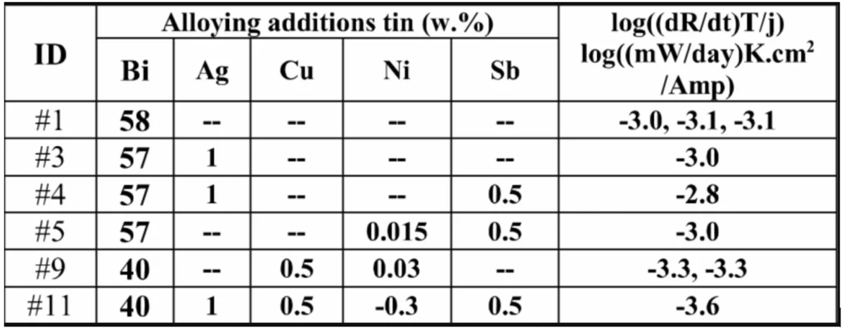
To combat the inherent brittleness of near-eutectic Sn-Bi solders (Sn58-Bi42), researchers are exploring the addition of dopants to improve mechanical properties. The iNEMI team has evaluated the effects of adding small concentrations of silver (Ag), copper (Cu), nickel (Ni), and antimony (Sb).
Interestingly, testing revealed that hypoeutectic alloys—those with lower bismuth content, such as 40% Bi and 60% Sn—exhibited better electromigration behavior than the standard eutectic 58% Bi alloy. The researchers concluded that because bismuth is the element dominating the electromigration process in these joints, simply reducing the bismuth content is more effective than adding complex alloying agents. These hypoeutectic solders offer a compromise: they maintain a lower reflow temperature than SAC305 while providing a more robust microstructure that is less prone to brittle fracture during drop-shock events.
Advanced Processing: Samsung’s Intense Pulsed Light (IPL) Method
Innovation in low-temperature soldering is not limited to material composition; it also extends to the soldering process itself. A research group from Samsung Electronics, led by Myeonng-Hyeon Yu, recently compared traditional reflow oven processing with Intense Pulsed Light (IPL) soldering.
IPL soldering utilizes high-intensity light to generate heat directly within the package via the photothermal effect. This method eliminates the need for long preheating cycles and significantly reduces the time the components spend above the melting point. Samsung’s findings suggest that IPL-soldered joints exhibit higher thermal cycling reliability than those processed in a reflow oven.
Specifically, in SAC305 joints, IPL-processed samples survived 1,900 thermal cycles compared to 1,200 for reflowed samples. The rapid cooling rate of the IPL method leads to the formation of smaller, more densely distributed Ag3Sn precipitates, which act as barriers to crack progression. When applied to LTS, this "hybrid" approach—using LTS paste with SAC305 balls—allows bismuth to diffuse more effectively, reinforcing the joint structure and mitigating CTE mismatches.
Strategic Applications: Silicon Photonics and Data Centers
The surge in AI data center buildouts has placed silicon photonics in the spotlight. These devices, which use light to transmit data at high speeds, are notoriously sensitive to the high temperatures of standard assembly. A reliability study led by Nokibul Islam and a team from STATS ChipPAC, JCET, and the Jiashan Fudan Institute compared Sn-Bi-Ag and Sn-Bi-Ag-Ni solders for photonics applications.
The team found that low-temperature solders produced significantly thinner intermetallic compounds (IMCs) than SAC305. Because IMC growth is a primary factor in solder joint degradation, the slower growth rates observed in LTS—particularly when used with copper/nickel-gold (Cu/NiAu) interfaces—suggest that LTS may be the superior choice for the 15-to-20-year lifespan required for infrastructure-grade photonics.
Conclusion and Future Outlook
The transition to low-temperature solders represents a strategic shift in semiconductor manufacturing rather than a mere material substitution. While SAC305 remains the "workhorse" for traditional applications and high-current-density HPC environments, its dominance is being challenged by the physical realities of modern packaging.
The industry’s path forward involves a tiered approach. Mobile and wearable devices, which prioritize thin profiles and energy efficiency, are already leading the adoption of Sn-Bi based solders. Meanwhile, the high-performance sector is carefully qualifying doped LTS alloys and hybrid soldering techniques to address the challenges of large-scale chiplet integration.
As package sizes continue to grow and the integration of optical and electronic components becomes standard, the ability to assemble these systems at lower temperatures will be a defining competitive advantage. Through continued collaboration between consortia like iNEMI and industry leaders like Samsung and Intel, the semiconductor sector is poised to overcome the reliability hurdles of tin-bismuth alloys, paving the way for a more sustainable and technologically capable era of electronics assembly.
