
As high-performance computing (HPC) and artificial intelligence (AI) accelerators push the boundaries of silicon density, the semiconductor industry has reached a critical juncture where thermal management is no longer a secondary design consideration but the primary bottleneck in system performance. The transition to 2.5D and 3D packaging, while essential for maintaining the scaling trajectory predicted by Moore’s Law, has introduced unprecedented multi-physics challenges. Modern packages, which integrate high-power Application-Specific Integrated Circuits (ASICs) with multiple High Bandwidth Memory (HBM) stacks on a silicon interposer, create a complex environment of tightly coupled thermal and mechanical interactions. To address these challenges, a new approach involving manufacturing-resolution geometry combined with deterministic, solver-accurate computation is redefining the economics and reliability of thermal analysis.
The Thermal Wall in High-Performance Computing
The rise of generative AI and large language models (LLMs) has necessitated a massive increase in computational throughput. This demand is met by packing more transistors into smaller footprints, leading to a surge in power density. Current state-of-the-art AI accelerators are now surpassing the 1 kW aggregate thermal design power (TDP) threshold. At these levels, the heat generated by the central ASIC is not the only concern; the proximity of HBM stacks creates a phenomenon known as die-to-die thermal crosstalk.
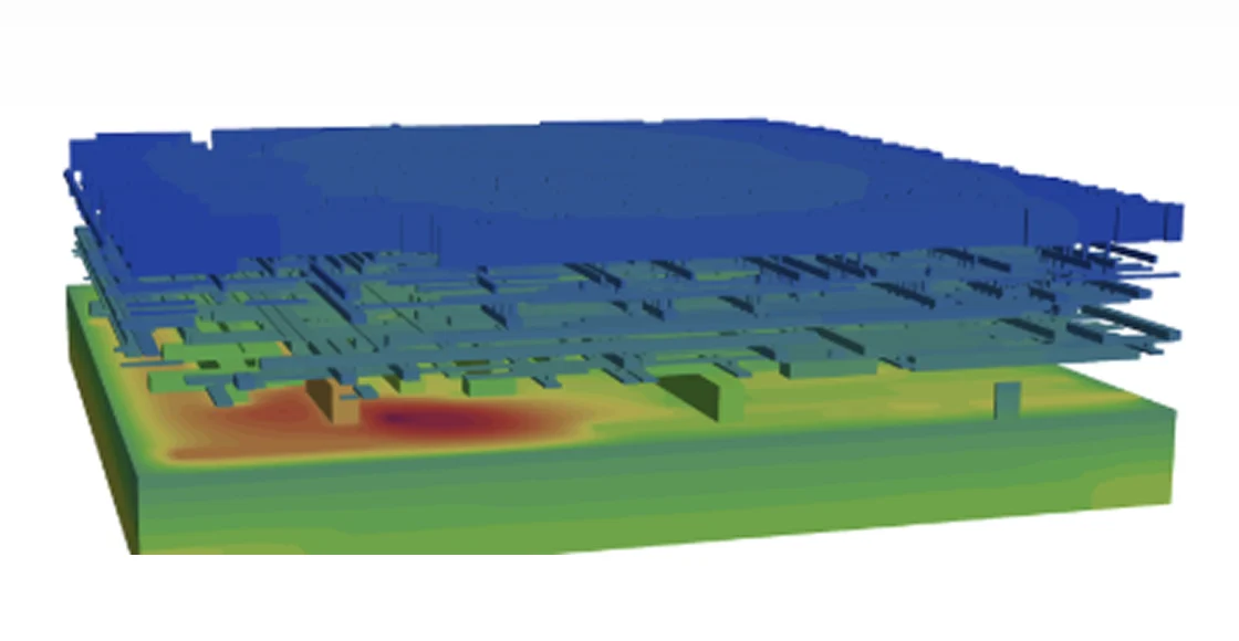
In a typical 2.5D configuration, the ASIC is surrounded by four, eight, or even twelve HBM stacks. As these memory stacks evolve from four or eight dies to 12 and 16 vertically stacked memory dies, the concentration of active silicon increases significantly. This vertical density creates a confined column of heat generation adjacent to the ASIC. When the ASIC runs at peak capacity, the heat bleeds across the silicon interposer, elevating the junction temperatures of the HBM dies. Because HBM performance and reliability are highly sensitive to temperature—often requiring operation below 95°C or 105°C to maintain data integrity—this thermal crosstalk can force a reduction in clock speeds, effectively throttling the system’s performance.
Architectural Complexity and the Warpage Challenge
Beyond simple temperature management, the mechanical integrity of the package is under constant threat from thermo-mechanical stress. A 2.5D package is a heterogeneous assembly of materials with vastly different Coefficients of Thermal Expansion (CTE). The silicon dies (CTE ~2.6 ppm/°C) are mounted on a silicon interposer, which is then attached to an organic substrate (CTE ~12–17 ppm/°C) and encapsulated in an epoxy molding compound (EMC).
During the reflow process and subsequent operational thermal cycling, these materials expand and contract at different rates. This mismatch drives "warpage"—a physical bowing of the package. Excessive warpage can lead to several catastrophic failure modes, including the cracking of the silicon interposer, delamination of the EMC, or the fracturing of micro-bumps and solder joints. As the industry moves toward larger package sizes (approaching 3x or 4x the reticle limit), the leverage of these CTE mismatches increases, making warpage prediction a prerequisite for manufacturing yield.
Limitations of Conventional Finite Element Analysis
For decades, Finite Element Analysis (FEA) has been the gold standard for structural and thermal simulation. However, the sheer complexity of modern 2.5D packages has exposed two fundamental limitations in conventional FEA workflows.

First, the "mesh bottleneck" prevents simulation at manufacturing resolution. To perform a standard FEA, the physical geometry must be discretized into a mesh of elements. A 2.5D package contains millions of distinct features: Through-Silicon Vias (TSVs), micro-bump arrays, and intricate Back-End-Of-Line (BEOL) metal layers. Creating a mesh that captures every individual TSV and metal trace would result in billions of degrees of freedom, exceeding the memory and processing capabilities of even the most advanced server clusters. Consequently, engineers are forced to "smear" or homogenize material properties—averaging the characteristics of the metal and dielectric layers—which sacrifices the ability to detect localized hotspots or fine-grained stress concentrations.
Second, the computational time required for high-fidelity FEA is incompatible with modern design cycles. A single high-resolution simulation can take days or even weeks to converge. In a fast-paced environment where design iterations happen daily, thermal analysis often becomes a "post-mortem" tool used to verify a finished design rather than a predictive tool used to guide the design process.
Vinci: A Paradigm Shift in Manufacturing-Resolution Simulation
The introduction of the Vinci system represents a departure from traditional homogenized simulation. By utilizing deterministic, solver-accurate physics computation directly on manufacturing-resolution geometry, Vinci eliminates the need for geometry simplification. This approach allows engineers to model the explicit representation of the multi-layer stackup, including every individual micro-bump and TSV.
This level of detail is critical because thermal behavior at the 16-die HBM level is governed by fine-grained spatial effects. Heat does not flow uniformly; it follows the path of least resistance through the vertical TSV columns and the horizontal BEOL metal traces. By simulating at manufacturing resolution, Vinci can capture tier-level hotspot formation within the HBM stack and the anisotropic resistance across the various layers. This ensures that the simulation reflects the actual physical hardware, providing a "digital twin" that is accurate enough to predict failures before a single prototype is manufactured.
Chronology of Thermal Management Evolution
The path to 1 kW+ packages has been marked by several distinct phases in packaging technology:
- The Monolithic Era (Pre-2015): Most high-performance chips were monolithic. Thermal management focused on the package lid and heat sink. Simulation was relatively straightforward as heat sources were localized to a single die.
- The Rise of 2.5D (2015–2020): The introduction of HBM1 and HBM2 necessitated the use of silicon interposers (e.g., TSMC’s CoWoS). Thermal crosstalk became a known issue, but power densities remained low enough that homogenized FEA models were sufficient.
- The Scaling Crisis (2021–2024): The jump to HBM3 and 12-die stacks increased the vertical height and power of memory components. Aggregate TDP reached 500W-700W. The industry began seeing "thermal-induced throttling" as a major hurdle in AI training clusters.
- The Manufacturing Resolution Era (2025–Present): With HBM3e and the upcoming HBM4 (featuring 16-die stacks and potentially 3D-stacked logic), the margin for error has vanished. Deterministic solvers like Vinci have emerged to provide the precision required for 1 kW+ designs.
Quantifying the Impact: Data and Reliability
The move to manufacturing-resolution simulation provides quantifiable benefits in both accuracy and time-to-market. In a representative 2.5D package evaluation, the use of deterministic solvers revealed temperature gradients within the HBM stack that were up to 15% higher than those predicted by homogenized models. This difference is the margin between a reliable product and one that fails in the field.
Furthermore, the ability to accurately predict thermo-mechanical warpage allows for the optimization of the epoxy molding compound and the substrate thickness early in the design phase. Data suggests that optimizing the "keep-out zones" around high-power TSVs can reduce localized stress by as much as 25%, significantly extending the fatigue life of the solder joints. By shifting the simulation earlier in the pipeline, companies can reduce the number of physical prototyping cycles, potentially saving millions of dollars in R&D costs.

Industry Reactions and Broader Implications
The shift toward high-resolution thermal analysis has drawn significant interest from the world’s leading foundries and fabless semiconductor companies. Analysts suggest that as the industry moves toward HBM4, the integration of memory and logic will become even more intimate, perhaps involving direct die-to-wafer bonding. In such scenarios, the thermal interfaces become even thinner, and the need for solver accuracy becomes even more acute.
"The economics of thermal analysis are changing," notes a senior packaging engineer familiar with the Vinci system. "We can no longer afford to be ‘mostly right’ about heat. If our simulation is off by five degrees, we lose 10% of our performance to throttling. If we are off on warpage, we lose our yield. Manufacturing-resolution geometry is the only way forward."
The implications of this technology extend beyond just GPUs and AI accelerators. As automotive SOCs (System on Chips) and telecommunications hardware adopt 2.5D packaging to handle 6G data rates and autonomous driving algorithms, the same thermal and mechanical rigors will apply. Reliability in these sectors is non-negotiable, and the ability to perform deterministic analysis at the level of individual vias and bumps will become a standard requirement for safety-critical hardware.
Conclusion: The Path Toward 2 kW and Beyond
As the industry looks toward the end of the decade, the roadmap for AI hardware suggests that 2 kW packages are on the horizon. Managing such extreme power levels will require not only advanced liquid cooling and backside power delivery but also a fundamental shift in how we simulate and validate these systems.
The transition from coarse, homogenized FEA to deterministic, manufacturing-resolution computation is a necessary evolution. By capturing the true complexity of the multi-layer stackup, systems like Vinci are enabling the next generation of HPC and AI accelerators to operate at peak performance without sacrificing long-term reliability. The integration of high-resolution geometry into the design flow ensures that the thermal and mechanical bottlenecks of today do not become the failures of tomorrow.
