
The semiconductor industry is currently undergoing a fundamental shift in design philosophy, transitioning from monolithic System-on-Chip (SoC) architectures toward disaggregated, chiplet-based systems. This evolution is driven by the escalating costs of leading-edge manufacturing nodes, the physical limits of reticle sizes, and the diverging development cycles of logic, memory, and analog components. While the initial adoption of chiplets was hindered by complex verification and packaging hurdles, the architecture has matured into a vital strategy for cost-effectively reusing intellectual property (IP) while maintaining compatibility with the latest high-speed input/output (I/O) protocols. As artificial intelligence (AI), machine learning (ML), and high-performance computing (HPC) demand unprecedented levels of bandwidth and processing power, chip architects are now faced with a critical strategic decision: which components of a system should remain stable, and which should be swapped to deliver the highest return on investment.
The Economic Drivers of Disaggregation
The primary catalyst for the chiplet movement is the sheer economic burden of advancing to sub-5nm process nodes. A standard monolithic tape-out at the 3nm or 2nm level can cost hundreds of millions of dollars, with mask sets alone accounting for a significant portion of that expenditure. In a monolithic design, every functional block—including those that do not benefit from scaling, such as analog I/O and power management—must be manufactured on the most expensive, leading-edge node. Chiplets break this requirement, allowing architects to place high-density logic on "bleeding-edge" nodes (N3 or N2) while keeping I/O and analog components on more mature, high-yield nodes like N7 or N12.
This modular recomposition allows for a more granular approach to product updates. Instead of a full multi-die respin, which carries immense risk and cost, a manufacturer can selectively update only the blocks that provide the greatest system-level benefit. This "mix-and-match" capability is becoming the standard for managing the rapid transitions in memory standards (such as the shift from LPDDR5X to LPDDR6) and interconnect protocols (such as the evolution of PCIe 5.0 to 6.0 and eventually 7.0).
Chronology of Chiplet Development and Standardization
The concept of combining multiple dies in a single package is not new, dating back to multi-chip modules (MCMs) used in the 1990s. However, the modern chiplet era began in earnest around 2017-2019, as companies like AMD utilized the Zen architecture to prove that disaggregated CPUs could outperform monolithic rivals in both yield and core count.
The timeline of the current ecosystem can be traced through several key milestones:
- 2019-2021: Early proprietary interconnects (like AMD’s Infinity Fabric) demonstrated the viability of the model but highlighted the need for industry-wide standards.
- 2022: The formation of the Universal Chiplet Interconnect Express (UCIe) consortium marked a turning point. This industry-standard provided a roadmap for a "plug-and-play" chiplet marketplace, backed by giants such as Intel, TSMC, Samsung, and ARM.
- 2023-2024: The explosion of Generative AI created a massive demand for HBM (High Bandwidth Memory) integration, forcing a rapid maturation of 2.5D and 3D packaging technologies like CoWoS (Chip on Wafer on Substrate).
- 2025 and Beyond: The industry is now moving toward UCIe 2.0 and Bunch of Wires (BoW) standards, focusing on stabilizing the die-to-die boundary to allow for the "swapping" strategies currently debated by architects.
The Strategy of Stability: Keeping I/O and Swapping Compute
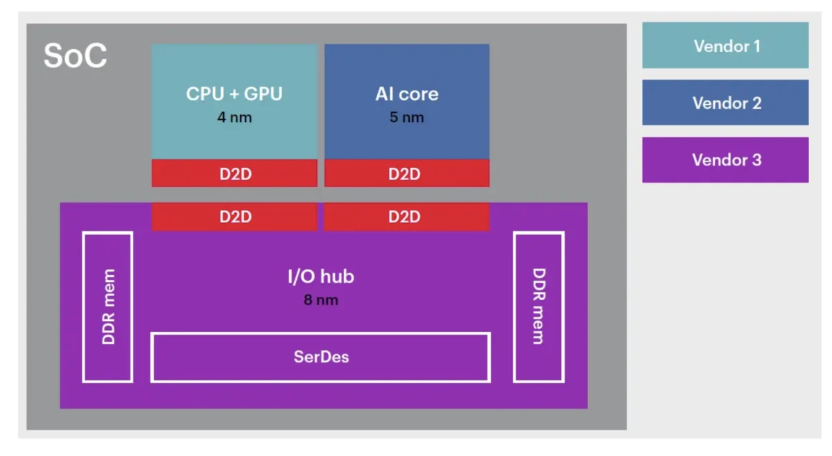
One of the most prominent strategies in the current market involves maintaining a stable I/O chiplet while upgrading the compute die. This approach is rooted in the "unromantic" reality of analog design. High-speed SerDes (Serializer/Deserializer) and physical layer (PHY) interfaces do not scale linearly with Moore’s Law. While a CPU’s logic density might double when moving from 7nm to 3nm, an analog PHY often sees little to no area reduction and may even face performance degradation due to the complexities of advanced FinFET or Gate-All-Around (GAA) transistors.
"In almost every case I can think of, the compute die is what rotates," noted Ashish Darbari, CEO of Axiomise. This makes economic sense because the compute die is where the architectural innovation happens—new AI accelerators, higher clock speeds, and improved instructions per cycle (IPC). Conversely, components like PCIe controllers, memory controllers, and security blocks mature slowly. By keeping these on a mature node, manufacturers avoid the "waste" of re-spinning a 224G SerDes on a 2nm process when a 5nm or 6nm implementation meets the specification at a fraction of the cost.
Furthermore, certification and qualification costs provide a strong incentive for I/O stability. In sectors like automotive and industrial automation, functional safety (FuSa) certifications are grueling and expensive. Redoing a certified I/O die simply to accommodate a new processor generation is often seen as commercially unviable.
The Strategy of Agility: Keeping Compute and Swapping I/O
Conversely, a growing contingent of architects argues that in the era of AI, I/O is the bottleneck that must be updated most frequently. As data centers transition to 800G and 1.6T Ethernet, the connectivity requirements of a cluster may evolve faster than the underlying compute architecture.

In this scenario, a "base" compute die—perhaps a high-performance NPU or GPU—remains the core of the product for several years, while different I/O chiplets are attached to tailor the product for specific markets. For example, a single compute die could be paired with a PCIe-heavy chiplet for server applications, an Ethernet-heavy chiplet for networking, or a specialized functional-safety chiplet for automotive use.
William Wang, CEO of ChipAgents, observed that in practice, I/O chiplets are often swapped more frequently because system requirements and connectivity standards are evolving at an unprecedented pace. Satish Radhakrishnan, head of GTM for semiconductor and electronics at Vinci, added that compute dies are so complex to redesign that architects are hesitant to touch them unless a massive performance leap is required. By absorbing new protocols into the cheaper, more easily updated I/O chiplets, companies can stay current with industry standards without the risk of a full processor redesign.
Technical and Integration Challenges
Regardless of which component is swapped, the integration of these dies presents significant engineering hurdles. The "brain versus limbs" analogy, popularized by Hee Soo Lee of Keysight EDA, illustrates the complexity: while it makes sense to keep the brain (compute) and swap the limbs (I/O) for different tasks, the nervous system (the interconnect) must be flawless.
Key technical challenges include:
- Thermal Management: Different chiplets on different nodes have different thermal profiles. A 3nm compute die generates intense localized heat, which can affect the performance of an adjacent analog I/O die.
- Power Integrity: Delivering clean power across a package to multiple dies with varying voltage requirements necessitates complex Power Delivery Networks (PDNs).
- Signal Integrity: As SerDes speeds reach 224 Gbps, the physical routing within the package becomes as difficult as traditional PCB routing. Any "swap" of a chiplet requires a full re-validation of the package-level signal integrity.
- Test and Observability: "Known Good Die" (KGD) testing is essential. If a manufacturer swaps a new I/O chiplet into an existing assembly and the system fails, they must be able to pinpoint whether the fault lies in the new die, the old die, or the interconnect.
Market Implications and Official Responses
The shift toward chiplet swapping is already reshaping the vendor-customer relationship. Companies like Cadence and Synopsys are seeing their customers move toward "disaggregated designs" where different parts of a system are built on different nodes to maximize yield. Arif Khan of Cadence noted that customers are increasingly looking for "advanced solutions they want to leverage for multiple generations," particularly in the AI data center space where "plumbing" (the interconnects) cannot be changed every year due to the length of the validation cycle.
In the commercial chiplet market, the dynamics differ from "captive" or vertically integrated systems. In a captive system (e.g., Apple or AWS), the manufacturer controls both dies and can synchronize their roadmaps. In the open market, however, the I/O die is often treated as a commodity that must remain stable to ensure compatibility with a wide range of third-party compute dies.
Future Outlook: The Rise of 3D-IC and Programmable I/O
Looking forward, the industry is exploring even more advanced configurations, such as 3D-IC, where chiplets are stacked vertically. This allows for a base die to provide foundational logic while specialized dies are "bonded" on top to add memory capacity or high-end features. While currently more difficult to manufacture due to hybrid bonding requirements, 3D stacking could eventually make the "swapping" process as simple as choosing a different top-layer die during the assembly phase.
Additionally, companies like Altera (an Intel company) are highlighting the role of programmable I/O. In industrial environments where dozens of different protocols (EtherCAT, Ethernet, etc.) are used, having a programmable interface allows for a "universal" chiplet that can be software-configured for different environments, further extending the life of the hardware.
Conclusion
The transition to chiplet-based architectures represents the semiconductor industry’s most significant adaptation to the post-Moore’s Law era. By treating silicon as a collection of modular building blocks rather than a single monolithic entity, architects have gained the flexibility to navigate a landscape of soaring costs and rapidly changing standards. Whether a company chooses to prioritize compute upgrades or I/O agility depends entirely on their specific market—be it the high-velocity world of AI data centers or the stability-focused realm of automotive electronics. As the ecosystem around standards like UCIe continues to mature, the ability to "swap and scale" will likely become the defining competitive advantage in chip design for the next decade.
