
The global semiconductor industry is currently navigating a period of unprecedented architectural transition, moving from traditional planar transistors to complex three-dimensional structures such as Gate-All-Around (GAA) FETs, Complementary FETs (CFETs), and vertical Gallium Nitride (GaN) power devices. As these architectures grow in complexity, the traditional reliance on physical wafer-based learning has become a significant bottleneck, inflating both Research and Development (R&D) costs and the critical time-to-market window. To address these challenges, Synopsys has introduced significant advancements to its Sentaurus Calibration Workbench (SCW), leveraging artificial intelligence (AI) and machine learning (ML) to transform Technology Computer-Aided Design (TCAD) from a qualitative research tool into a predictive engine for high-volume manufacturing.
The core issue facing modern semiconductor fabrication is the linear and iterative nature of wafer-based learning. In this traditional model, engineers must fabricate a physical wafer, measure its performance, and then adjust process parameters for the next run. Given that a single advanced logic wafer can take several months to traverse the cleanroom and cost tens of thousands of dollars, this "trial and error" approach is increasingly unsustainable. TCAD serves as the digital twin of the fabrication facility, using sophisticated physics-based models to simulate the effects of various process steps—such as ion implantation, annealing, and etching—on the final device performance. However, for TCAD to be effective, it must be "calibrated" so that its virtual results mirror the physical reality of the silicon produced in a specific fab.
The Evolution of TCAD Calibration and the Role of SCW
Historically, TCAD calibration was a manual, labor-intensive process reserved for expert physicists. Engineers would manually tune hundreds of physical model parameters—ranging from carrier mobility to defect recombination rates—until the simulation curves matched the electrical data from test wafers. This process often took weeks or even months, frequently lagging behind the rapid pace of process development. By the time a model was calibrated, the process recipe had often already changed, rendering the model obsolete for predictive use.
The introduction of the Sentaurus Calibration Workbench (SCW) marked a pivotal shift in this chronology. SCW was designed to provide an end-to-end environment for managing the calibration workflow, integrating process and device simulation tools with a robust graphical user interface (GUI). The latest iteration of SCW addresses the "expertise gap" by incorporating AI-driven automation. Instead of executing one simulation at a time, SCW now executes multiple parallel simulations to build a comprehensive ML model of the device behavior. This shift allows for rapid inference, enabling engineers to find the optimal set of calibration parameters in a fraction of the time previously required.
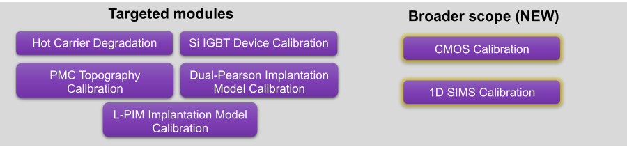
Strategic Enhancements: Expert Modules and Productivity Gains
One of the most significant updates to the Synopsys TCAD suite is the introduction of expert-curated calibration modules. These modules are designed to provide a 5X productivity boost by offering pre-built workflows for specific, high-demand use cases. In the early stages of technology pathfinding, where fabs are evaluating competing architectures like Si CFET versus 3D CMOS image sensors, these modules allow teams to start with 80% of their workflow already established.

These modules cover a broad spectrum of applications, including:
- CMOS Calibration: Tailored for advanced logic nodes where short-channel effects and parasitic capacitance are dominant.
- SIMS (Secondary Ion Mass Spectroscopy) Calibration: Focused on the precise modeling of dopant profiles, which is essential for defining junction depths in sub-7nm nodes.
- Vertical GaN and Power Electronics: Optimized for wide-bandgap materials where thermal management and breakdown voltage are critical design constraints.
By providing these internal baselines, Synopsys enables different teams within a semiconductor company to share and reuse calibration data. This collaborative approach ensures that the knowledge gained during the R&D phase is preserved and utilized as the technology moves toward product ramp and high-volume manufacturing.
Technical Analysis of ML Enhancements and UANN Integration
Beyond the pre-built modules, Synopsys has integrated advanced machine learning technology blocks that allow expert users to construct their own customized workflows. A key feature in this category is the optimization of the Design of Experiments (DOE). In TCAD, a DOE is a set of simulation runs used to map out the design space. Traditionally, DOEs were populated via random sampling, which often required a large number of simulations to achieve accuracy.
The new SCW update utilizes "Active Learning" via a "query by committee" approach. This method interactively populates the DOE by identifying areas of the design space where the ML model has the highest uncertainty and focusing subsequent simulations on those areas. Data suggests that Active Learning can achieve the same level of model accuracy as random sampling while using up to 50% fewer DOE runs. Furthermore, features such as weighted and hypersphere sampling allow engineers to prioritize high-value data points and filter out outliers that might otherwise skew the calibration.
A groundbreaking development in this release is the implementation of Uncertainty-Aware Neural Networks (UANNs). Semiconductor data is notoriously non-uniform; certain process conditions are well-characterized, while others remain sparse. UANNs are uniquely suited for this environment because they provide a measure of confidence for every prediction they make. From a computational standpoint, UANNs offer a 5X faster training time compared to traditional Gaussian process networks. They also simplify the workflow for TCAD engineers by removing the need for the traditional "train-test-validate" cycle of standard ML development. The efficiency gains are measurable: UANNs have been shown to reduce DOE consumption by 15% for device simulation and by as much as 70% for topography simulation in tools like Sentaurus Topography.
Scaling Computational Power: The ML Calibration Accelerator
As semiconductor designs move toward full 3D integration, the computational load required for simulation increases exponentially. To prevent the simulation itself from becoming a bottleneck, Synopsys has launched the Sentaurus ML Calibration Accelerator. This companion product is designed to scale compute resources specifically for ML-based workflows.

The accelerator employs a stackable licensing model, allowing fabs to allocate additional compute power to particularly demanding tasks, such as the calibration of 3D NAND strings or complex SRAM bitcells. According to Synopsys data, the ML Calibration Accelerator delivers a greater than 5X reduction in total calibration turnaround time. Because it is designed to work "out of the box" with existing SCW workflows, it provides a seamless path for engineers to move from data collection to predictive modeling within a matter of days.
Industry Implications and the Path to "Virtual Fabs"
The implications of these advancements extend far beyond the productivity of individual TCAD engineers. In the broader context of the global semiconductor race, the ability to calibrate models rapidly is a strategic advantage. Major foundries and Integrated Device Manufacturers (IDMs) are under intense pressure to yield silicon on new nodes faster than ever before.
Industry analysts suggest that the integration of AI into TCAD workflows is a necessary step toward the realization of the "Virtual Fab." In this vision, a significant portion of process optimization—traditionally done on the factory floor—is moved into a simulated environment. By reducing the number of physical test wafers required for development, companies can save hundreds of millions of dollars in R&D costs and significantly reduce the carbon footprint associated with semiconductor manufacturing.
Furthermore, the accuracy of these calibrated models is critical for the "Design-Technology Co-Optimization" (DTCO) process. As the margins for error shrink at the 3nm and 2nm nodes, the interaction between the physical process and the circuit design becomes more pronounced. Calibrated TCAD models provide the parasitic information and device characteristics necessary for designers to optimize chip performance long before the first production wafer is ever patterned.
Conclusion and Future Outlook
The latest updates to the Synopsys Sentaurus Calibration Workbench represent a significant milestone in the application of AI to semiconductor manufacturing. By combining expert modules, active learning, UANNs, and hardware acceleration, Synopsys has addressed the primary hurdles to TCAD adoption: complexity and time.
The data indicates a clear trend: a cumulative productivity boost of over 5X in workflow creation and a subsequent 5X acceleration in execution. For the semiconductor industry, this means that TCAD calibration, once a months-long endeavor, can now be completed in days. As the industry looks toward the next frontier of innovation—including chiplets, heterogenous integration, and 2D materials—the role of AI-driven simulation will only become more central. The ability to bridge the gap between virtual models and physical hardware with speed and precision is no longer just an efficiency gain; it is a fundamental requirement for the future of silicon development.
