

The rapid evolution of high-performance computing (HPC), artificial intelligence (AI), and automotive electronics has placed unprecedented demands on the semiconductor packaging industry. As chip architectures become more complex and power densities rise, the management of thermal energy has emerged as a primary bottleneck in device reliability and performance. To address these challenges, the industry is increasingly turning to advanced materials and simulation-driven design. However, a significant gap has emerged between theoretical simulations and the physical behavior of new materials, specifically Metal Thermal Interface Materials (TIMs). A recent comprehensive study by researchers at Amkor Technology Korea—including Dambi Jo, JiHyun Kim, and KyungRok Park—has identified critical discrepancies in traditional simulation models and proposed a new methodology for characterizing material properties that aligns virtual predictions with real-world performance.
The Strategic Importance of Thermal Management in the AI Era
In the current semiconductor landscape, the transition from polymer-based TIMs to metal-based alternatives is driven by the need for superior thermal conductivity. High-performance packages generate significant localized heat; if this heat is not dissipated efficiently, it can lead to thermal throttling, reduced lifespan, or catastrophic failure of the silicon die. Metal TIMs, such as Indium-Silver alloys, offer significantly higher thermal conductivity than conventional polymer-based gels or adhesives.
Despite these advantages, the integration of metal TIMs introduces mechanical complexities. The semiconductor industry relies heavily on finite element analysis (FEA) to predict warpage and stress before a single physical prototype is built. This simulation-first approach is essential for minimizing the exorbitant costs and lengthy timelines associated with modern package fabrication. As packages grow in size and complexity—utilizing technologies like Flip Chip Ball Grid Array (FCBGA) and lidded structures—the accuracy of these simulations becomes a financial and operational imperative. When simulations fail to predict actual warpage, the resulting design iterations can cost companies millions of dollars in lost time and material waste.

The Discrepancy Between Bulk Properties and Thin-Film Reality
The core challenge identified in the Amkor study involves the material property data used in simulations. Traditionally, engineers utilize material properties provided by suppliers, which are typically derived from "bulk" specimens—often large, dog-bone-shaped samples used in standard tensile testing. For metal TIMs, these bulk measurements often suggest a high elastic modulus, such as the 15.5 gigapascals (GPa) reported for certain Indium-Silver alloys.
However, in a real-world semiconductor package, the metal TIM does not exist in a bulk state. Instead, it is applied as an extremely thin film, often less than 0.5 mm thick, sandwiched between a silicon die and a protective lid. The researchers found that applying bulk-derived properties to thin-film simulations resulted in significant errors. While polymer TIMs, which have decades of accumulated data, show a high correlation between simulation and reality, metal TIMs are relatively new to high-volume manufacturing, and their thin-film mechanical behavior is not yet fully characterized by standard supplier data sheets.

Experimental Methodology: Shadow Moiré and Test Vehicle Construction
To bridge this gap, the research team fabricated a lidded FCBGA test vehicle (TV) to serve as a baseline for comparison. The metal TIM test vehicle featured a 25.6 mm x 25.6 mm die with a thickness of 0.55 mm, utilizing a 0.4 mm thick Indium 10 Silver (In10Ag) preform. For comparison, a polymer TIM test vehicle was also constructed using a 0.78 mm thick die and a 0.07 mm thick gel-type polymer TIM.
The primary tool for measuring physical behavior was the shadow moiré system. This technique, governed by the JEDEC JESD22-B112 standard, allows for the quantitative analysis of package warpage across a wide temperature range. By increasing temperatures from 25°C to 260°C at a controlled rate of 5°C per minute, the researchers could observe how the package deformed during conditions mimicking the reflow soldering process.

The study tracked the packages through two critical stages:
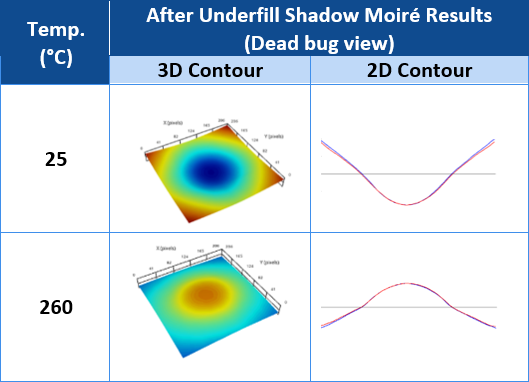
- After-Underfill (AUF): The state after the die is attached and the underfill is cured, but before the TIM and lid are applied.
- End-of-Line (EOL): The final state of the package, including the TIM, lid, and lid adhesive.
Chronology of Findings: The Warpage Transition
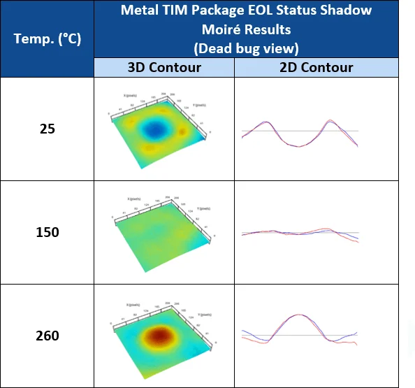
The shadow moiré tests revealed a complex "warpage signature" for both package types. In the AUF state, both metal and polymer packages exhibited "crying mode" (concave) warpage at room temperature, which transitioned to "smile mode" (convex) at elevated temperatures. This behavior was expected and easily replicated in initial simulations.

However, the results diverged significantly at the EOL stage. Physical measurements showed that both metal and polymer TIM packages developed a "W-shaped" warpage profile at room temperature and an "M-shaped" profile at high temperatures. Both packages reached a relatively flat, deformation-free state at approximately 150°C.
When these scenarios were simulated using supplier-provided bulk material properties, the polymer TIM simulation showed an excellent match with the physical results. In contrast, the metal TIM simulation failed spectacularly. Instead of the observed "W-shape" at room temperature, the simulation predicted a simple "smile-mode" warpage. This discrepancy confirmed that the 15.5 GPa elastic modulus derived from bulk specimens was fundamentally unsuitable for modeling the behavior of the metal TIM as a thin film within the package.

Redefining Material Characterization: The Rheometer Breakthrough
Seeking a more accurate way to model the metal TIM, the researchers conducted a battery of material characterization tests on actual film-type specimens. These included:
- Tensile Testing: Traditional stretching of the material.
- Dynamic Mechanical Analysis (DMA): Measuring stiffness and damping.
- Nano-indentation: Testing hardness at the microscopic level.
- Rheometer Testing: Measuring how the material flows and deforms under applied stress.
While tensile testing and DMA continued to yield high modulus values similar to the supplier’s bulk data, the rheometer test produced a breakthrough. The rheometer-derived modulus was significantly lower than the bulk values. The reason for this difference lies in the nature of the test: the rheometer applies force in a manner that mimics the vertical and directional stresses the TIM experiences during package assembly and thermal cycling. Unlike a dog-bone specimen being pulled apart, the rheometer accounts for the process-induced effects and the geometric constraints of a thin film.

Validation and Correlation
When the researchers replaced the bulk-derived modulus with the rheometer-derived modulus in their simulation models, the results aligned with the shadow moiré data. The updated simulation accurately captured the absolute warpage values across the 25°C to 260°C range. More importantly, it successfully reproduced the complex transition from "W-shaped" to "M-shaped" warpage.
This correlation provides a definitive empirical foundation for future package design. It proves that for advanced metal TIMs, the "process-effect" is just as important as the raw material composition. The mechanical properties of the material are not static; they are influenced by the thickness of the application and the directional forces applied during the bonding process.

Industry Implications and Future Outlook
The implications of this research for the semiconductor industry are profound. As the sector moves toward 2.5D and 3D packaging architectures to support AI workloads, the margin for error in thermal and mechanical design is shrinking.
- Cost Reduction: By identifying the rheometer as the most accurate testing method for TIM simulations, manufacturers can reduce the number of physical "build-and-test" cycles. This can shave months off the development timeline for new chipsets.
- Design Reliability: Accurate warpage prediction is critical for ensuring long-term solder joint reliability. If a package warps more than predicted, it can lead to "bridge" defects or open circuits during board-level assembly.
- Material Innovation: This study opens the door for the optimization of other metal TIM compositions. The research team has already indicated that future work will extend to Indium-Silver alloys with different ratios and copper-based TIMs, using the same rheometer-based simulation validation.
- Standardization: There is now a clear case for updating industry standards regarding how material properties are reported by suppliers. Providing thin-film properties alongside bulk data could become a new requirement for the high-performance packaging supply chain.
Conclusion
The work of the Amkor Technology Korea team serves as a critical course correction for semiconductor mechanical engineering. As the industry pushes the boundaries of what is possible with metal TIMs in AI and automotive applications, the reliance on legacy bulk material data is no longer tenable. By shifting to characterization methods like rheometer testing that reflect actual application conditions, engineers can finally achieve the high-fidelity simulations required for the next generation of high-performance electronics. This research not only enhances design reliability but also reinforces the vital link between material science and virtual prototyping in the quest for more efficient, more powerful, and more reliable semiconductor solutions.
