
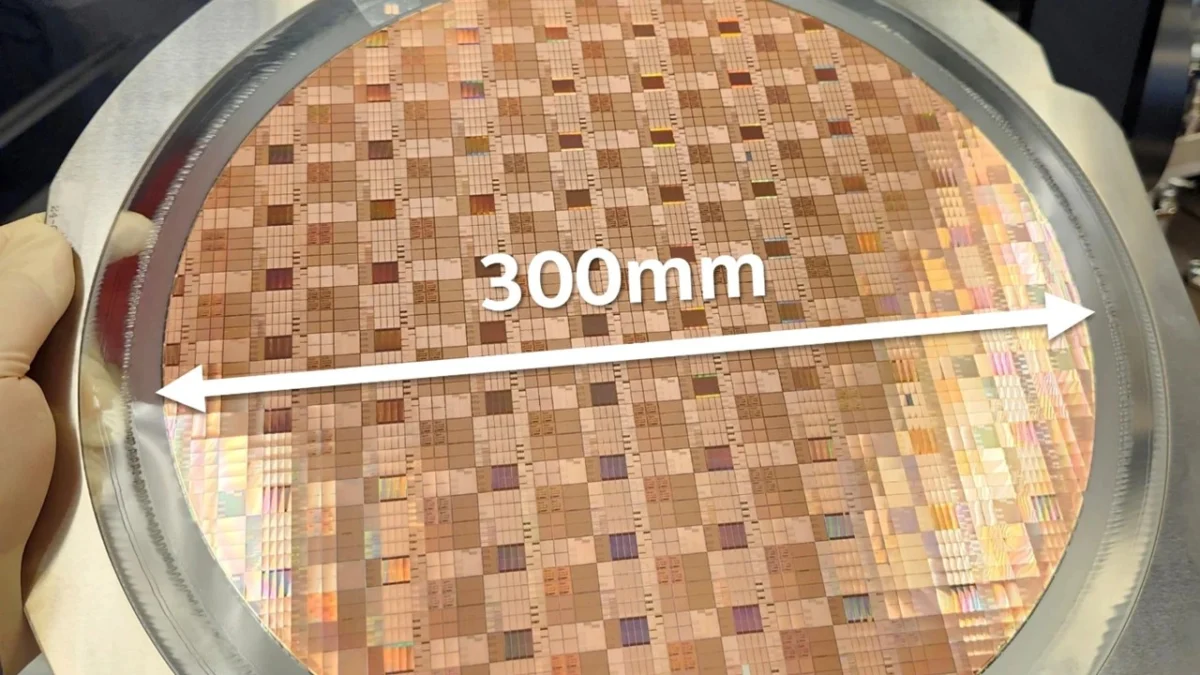
Researchers at Intel Foundry have demonstrated a groundbreaking gallium nitride (GaN) chiplet technology manufactured on 300 mm GaN-on-silicon wafers, representing a major technical milestone in the evolution of power electronics and high-frequency communications. This advancement, detailed at the 2025 IEEE International Electron Devices Meeting (IEDM), addresses the critical limitations of traditional silicon-based semiconductors as the industry enters an era of hyper-scale data centers and 6G wireless connectivity. The Intel Foundry team successfully produced an ultra-thin GaN chiplet with a base silicon substrate measuring only 19 micrometers (µm) thick—roughly one-fifth the diameter of a human hair—while achieving the industry’s first monolithic integration of digital control circuits on the same die. This unified manufacturing process eliminates the historical trade-offs between power density, switching speed, and physical footprint, positioning Intel at the forefront of the post-silicon power revolution.
The emergence of this technology comes at a pivotal moment for the global semiconductor industry. As graphics processing units (GPUs) for artificial intelligence and high-performance computing (HPC) servers demand increasingly higher power levels in ever-shrinking chassis, traditional silicon (Si) power management components have reached their physical threshold. Silicon’s inherent material properties limit its efficiency at high voltages and its ability to dissipate heat in compact environments. By contrast, gallium nitride is a wide-bandgap semiconductor capable of handling higher electric fields and faster switching speeds with significantly lower energy loss. Intel’s breakthrough lies not just in the material itself, but in the ability to manufacture these high-performance GaN chiplets at scale using standard 300 mm (12-inch) wafer infrastructure, which drastically improves the economic viability of the technology compared to smaller, more expensive 150 mm or 200 mm wafer formats.
The Material Advantage: Why GaN is the Future of Power
To understand the significance of Intel’s achievement, one must examine the physics of gallium nitride. As a compound semiconductor, GaN possesses a "wide bandgap," which refers to the energy required to free an electron from its orbit around an atom so it can conduct electricity. Silicon has a bandgap of approximately 1.1 electron volts (eV), whereas GaN’s bandgap is roughly 3.4 eV. This larger gap allows GaN devices to withstand much higher voltages before breaking down and enables them to operate at significantly higher temperatures—often exceeding 200°C—where silicon would typically fail.
Furthermore, GaN transistors exhibit much higher electron mobility than silicon. In practical terms, this means they can switch on and off at frequencies in the gigahertz range with minimal resistance. This high-frequency capability is essential for modern power conversion, where faster switching allows for the use of smaller inductors and capacitors, leading to more compact power supplies. In the context of wireless infrastructure, this allows for the creation of radio frequency (RF) frontends that can handle the massive bandwidth requirements of 5G and the emerging 6G standards, which are expected to utilize the centimeter- and millimeter-wave bands.

Engineering the World’s Thinnest GaN Chiplet
The physical miniaturization of the GaN chiplet was achieved through a sophisticated engineering process known as Stealth Dicing Before Grinding (SDBG). Typically, thinning a 300 mm wafer is a high-risk operation because the mechanical stress can shatter the brittle GaN layers or damage the intricate metal wiring of the transistors. The Intel Foundry team utilized a precisely tuned laser to create microscopic fracture lines deep within the silicon substrate. Once these internal "perforations" were established, the wafer underwent a mechanical grinding process to reduce its thickness to the 19 µm target.
The result is a chiplet that is not only thin but also exceptionally robust. Intel’s testing verified that the thinning process did not degrade the electrical characteristics of the transistors. Devices with gate lengths as small as 30 nanometers (nm) demonstrated the ability to block up to 78 volts while maintaining high current-carrying capacity. For RF applications, the transistors achieved cut-off frequencies exceeding 300 GHz, a benchmark that places this technology in the upper echelon of semiconductor performance for future telecommunications hardware.
Monolithic Integration: The End of the Companion Chip
Perhaps the most significant innovation presented at IEDM 2025 is the integration of silicon logic directly onto the GaN chiplet. In current industry designs, a GaN power transistor usually requires a separate silicon-based "driver" chip to control its switching behavior. This "two-chip" solution introduces parasitic inductance—a phenomenon where energy is lost as signals travel through the wires connecting the two components.
Intel solved this by using a "layer transfer" process to place silicon p-channel metal-oxide-semiconductor field-effect (Si PMOS) transistors side-by-side with GaN N-channel metal-oxide-semiconductor high-electron-mobility transistors (N-MOSHEMT) on the same die. This creates a fully monolithic system where the digital control logic and the power delivery components share the same wiring layers.
The research team successfully built a complete library of digital building blocks using this combined process, including NAND gates, multiplexers, and ring oscillators. Speed measurements showed that inverters switched in a mere 33 picoseconds. The uniformity of these results across the entire 300 mm wafer suggests that the process is ready for high-volume manufacturing, a hurdle that has stymied previous attempts at GaN-silicon integration.

Chronology and Development Timeline
The journey to the 300 mm GaN-on-silicon platform has been a multi-year endeavor for Intel Foundry.
- 2020–2022: Initial research focused on the feasibility of growing high-quality GaN crystal layers on large-diameter silicon wafers, overcoming the "lattice mismatch" that often causes wafers to bow or crack.
- 2023: Intel demonstrated early prototypes of GaN power transistors on 300 mm wafers, proving that the material could be processed in existing high-volume CMOS foundries.
- 2024: The focus shifted to miniaturization and integration, leading to the development of the SDBG technique and the first successful layer transfers of silicon PMOS onto GaN substrates.
- 2025: Presentation at IEDM of the fully integrated, 19 µm thin chiplet, marking the transition from laboratory research to a viable product platform.
Industry Implications and Reliability Standards
The transition to a 300 mm GaN platform has profound economic implications. By using standard 12-inch wafers, Intel can produce more than twice as many chips per wafer compared to the 200 mm (8-inch) wafers used by many competitors. This economies-of-scale advantage is expected to drive down the cost of GaN technology, making it accessible not just for high-end aerospace and defense applications, but for consumer electronics and electric vehicles (EVs).
In the automotive sector, GaN’s efficiency could translate into faster charging times and longer range for EVs by reducing the weight and size of the onboard power electronics. In data centers, the ability to place voltage regulators closer to the CPU or GPU—enabled by the thinness and efficiency of these chiplets—could reduce "power delivery network" losses by up to 30%, saving millions of dollars in electricity costs for hyperscale operators like Microsoft, Google, and Amazon.
Intel also addressed the skepticism surrounding GaN’s long-term durability. The research team subjected the new chiplets to four rigorous industry-standard reliability tests:
- Time-Dependent Dielectric Breakdown (TDDB): To ensure the insulating layers do not fail under constant voltage.
- Positive Bias Temperature Instability (pBTI): To test the stability of the transistor’s threshold voltage over time.
- High-Temperature Reverse Bias (HTRB): To simulate the stress of blocking high voltages in hot environments.
- Hot-Carrier Injection (HCI): To measure the impact of high-energy electrons on the device’s lifespan.
The chiplets met or exceeded all required metrics, providing the "industrial-grade" assurance necessary for deployment in mission-critical infrastructure.

Analysis: A Strategic Pivot for Intel Foundry
Industry analysts view this breakthrough as a strategic move to diversify Intel’s foundry offerings. As the company competes for external customers through its Intel Foundry business unit, the ability to offer a "GaN-as-a-Service" platform on 300 mm wafers provides a unique selling point that many traditional silicon foundries cannot yet match.
The integration of GaN and silicon on a single chiplet aligns with the broader industry trend toward "chiplet-based architectures," where different functions (logic, memory, and power) are broken into optimized pieces and reassembled in a single package. Intel’s work suggests a future where a single high-performance package could contain an AI processor, high-bandwidth memory, and a GaN-based power delivery system, all operating with unprecedented synergy.
As the semiconductor world moves toward the 2030s, the demand for energy-efficient computing will only intensify. Intel’s 300 mm GaN-on-silicon platform provides a roadmap for meeting that demand, offering a combination of performance, scale, and reliability that could redefine the boundaries of electronic design. With the successful demonstration of the world’s thinnest GaN chiplet, the path is now clear for the next generation of more powerful, more efficient, and more compact digital systems.
