

The global semiconductor industry is currently navigating a pivotal transition where artificial intelligence, high-performance computing, and advanced manufacturing processes are converging to redefine the capabilities of essential modern technologies. At the center of this evolution is a strategic shift toward chiplet-based architectures and collaborative co-development models aimed at overcoming the physical and economic barriers of sub-2nm fabrication. As engineering requirements for medical devices, electric vehicles (EVs), and humanoid robots become increasingly stringent, the industry is moving away from siloed innovation toward a shared technological DNA that leverages economies of scale across disparate sectors.
The Lithography Bottleneck and the Rise of Reticle Stitching
As the industry pushes toward the sub-2nm frontier, the physical limitations of existing lithography tools have become a primary concern for chip designers. Traditionally, the lithography exposure field is constrained by the size of the reticle, which is standardly 26 x 33 mm. This "reticle limit" effectively caps the size of a monolithic System-on-Chip (SoC), posing a significant challenge for high-performance computing (HPC) and AI applications that require massive die areas to house billions of transistors.
To circumvent this, engineers are increasingly turning to reticle stitching. This technique involves running patterns across the edge of the reticle to join two adjacent exposure fields, essentially forming a single, larger chip from multiple exposures. However, this process is fraught with technical hurdles. Germain Fenger, Senior Director of Product Management at Synopsys, notes that field edges introduce significant distortions that can compromise imaging integrity. Because these borders now appear in the middle of the functional chip rather than at the periphery, designers must use Inverse Lithography Technology (ILT) and Optical Proximity Correction (OPC) to mitigate these effects.

ILT, a computationally intensive process, produces complex, curved features on the mask to compensate for optical distortions, ultimately resulting in the desired straight lines on the silicon wafer. At research hubs like imec, these tools are being validated to ensure that modified design rules can be applied locally at the stitch points, allowing for seamless connectivity across the die without sacrificing performance or yield.
Vertical Integration and the Software-Defined Vehicle
The automotive sector is perhaps the most visible beneficiary of these semiconductor advancements. The transition from internal combustion engines to electric, autonomous platforms has fundamentally changed the bill of materials for modern vehicles. By 2030, electronics are expected to account for approximately 50% of a car’s total cost, reflecting a massive surge in software complexity and processing requirements.
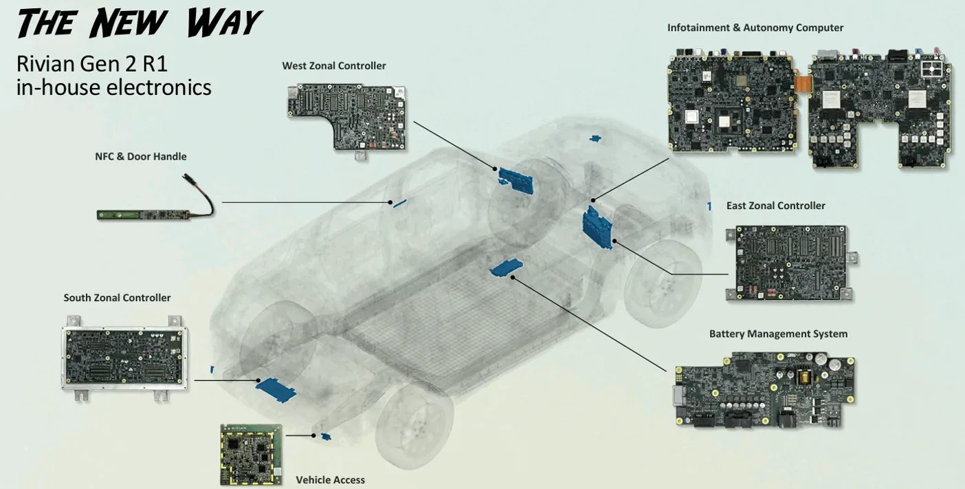
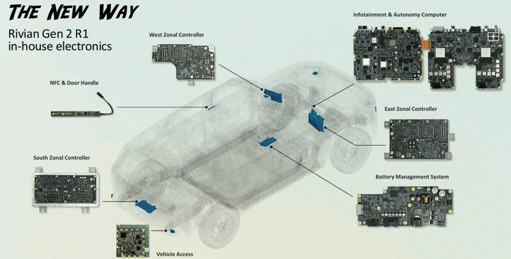
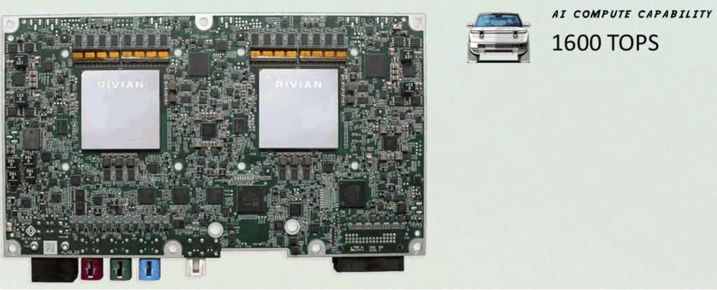
Rivian, a leader in the EV space, has demonstrated the power of vertical integration by moving away from the traditional Tier 1 supplier model. In the past, original equipment manufacturers (OEMs) acted primarily as integrators, piecing together 40 to 100 disparate Electronic Control Units (ECUs) from various vendors. Rivian’s approach treats the vehicle as a single, networked computer. Their first-generation autonomy processor, the RAP1, is a custom 5nm SoC manufactured by TSMC, integrated with three High Bandwidth Memory (HBM) stacks.
Vidya Rajagopalan, Senior Vice President of Electrical Hardware at Rivian, emphasizes that this "clean sheet" approach allowed the company to simplify its electronic architecture into a handful of zonal Printed Circuit Boards (PCBs). This move toward multichip modules (MCMs) that combine memory, SoCs, and power management into sophisticated packages is a trend likely to be adopted by more Western and Chinese manufacturers seeking to reduce latency and improve the determinism required for physical AI in self-driving systems.
The Autonomous Edge Chiplet Program and Global Standardization
The economic reality of the automotive market—where vehicle volumes are relatively flat compared to consumer electronics—requires a new approach to research and development. While roughly 96.4 million vehicles were produced globally in 2025, the exponential demand for compute power in these vehicles cannot be met through traditional linear market growth.
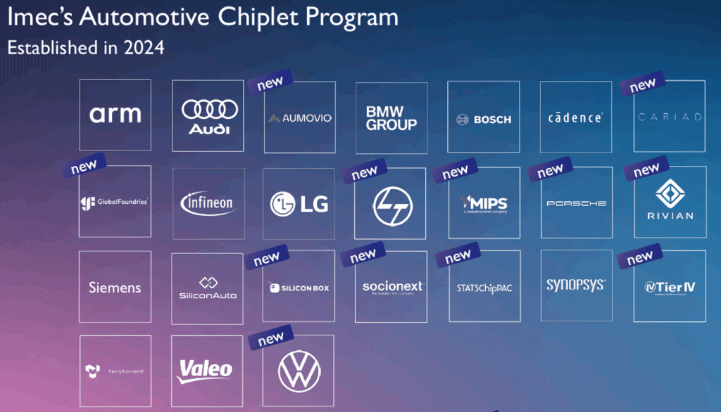
In response, imec recently renamed and expanded its efforts into the Autonomous Edge Chiplet Program (AECP). This initiative builds upon the Automotive Chiplet Program (ACP) launched in 2024, which currently includes 24 members ranging from OEMs and semiconductor manufacturers to EDA (Electronic Design Automation) firms and OSATs (Outsourced Semiconductor Assembly and Test). A key component of this effort is the new chiplet acceleration center in Heilbronn, Germany, which focuses on prototyping and de-risking the adoption of chiplets for industrial use.
The AECP aims to create a reference platform within the next 12 months that prioritizes interoperability among chiplets from different vendors. This is not merely a European endeavor; imec is collaborating with Japan’s Advanced SoC Research for Automotive (ASRA) to harmonize architecture specifications. By creating a "common architectural DNA," the industry hopes to reuse technologies developed for automotive applications in other sectors, such as drones and industrial automation, thereby reducing costs and accelerating time-to-market.
Repurposing Semiconductor Tech for Breakthrough Medical Diagnostics
Beyond transportation, semiconductor innovations are making profound inroads into healthcare. Hyperspectral imaging, a technology originally developed for satellite and industrial applications, is now being integrated into CMOS image sensors for medical use. By depositing optical filters directly onto pixels with lithographic precision, researchers can capture the unique "spectral signature" of different materials.
In surgical settings, this technology allows doctors to distinguish between healthy and diseased tissue in real-time. Hypervision Surgical, a pioneer in this field, uses hyperspectral cameras to detect oxygen saturation levels, helping surgeons identify tissue at risk of ischemia. Furthermore, this non-invasive imaging is being tested as a diagnostic tool for the retina to identify early-stage signatures of neurodegenerative conditions like Alzheimer’s and Parkinson’s diseases long before physical symptoms appear.
The role of AI in medicine is also evolving to address data loss. Dan Wattendorf of the Gates Foundation points out that traditional medical readings, such as EKGs or Complete Blood Counts (CBCs), often undergo extreme data compression. For example, a CBC compresses 9 million data points into just 20 numbers for physician review. By applying machine learning to uncompressed, raw waveforms, researchers are discovering "hidden" data that can predict structural heart defects or historical atrial fibrillation that no human clinician could detect.
Physical AI and the Efficiency of Humanoid Robotics
The rise of humanoid robots represents the next frontier for "Physical AI," a field where latency and energy efficiency are more critical than raw processing power. Unlike generative AI, which can tolerate slight delays in response, a robot interacting with the physical world requires deterministic, real-time performance to ensure safety and balance.
Salil Raje, Senior Vice President at AMD, notes that the architecture of a humanoid robot mirrors a biological system: a central "brain" for planning, a synchronous "spine" (often a time-sensitive network) for coordination, and "limbs" for local actuation. To manage the massive data flow from hundreds of sensors, developers are moving toward local data encoding. By filtering and resizing data at the source and sending only "tokens" or insights to the central brain, data traffic can be improved by two to three orders of magnitude.
Energy efficiency remains the primary hurdle. Ahmed Bahai, CTO of Texas Instruments, argues that the industry must look toward bio-inspired technologies. The human brain is estimated to be 10,000 times more efficient than any current silicon-based device. This has led to the exploration of Sensory Language Models (SLMs) rather than Large Language Models (LLMs). SLMs aim to mimic the way a human infant learns—using intuition and minimal data points to build a vocabulary of movement and interaction—which is far more power-efficient for edge-based AI applications.
Conclusion: A Future Built on Collaborative Ecosystems
The complexity of sub-2nm processing and advanced 3D packaging has reached a point where no single company can maintain a leadership position in isolation. The progress detailed at the imec International Technology Forum highlights a future defined by "co-development," where material scientists, lithographers, and end-market engineers work in parallel full-process flows.
The transition from the Automotive Chiplet Program to the broader Autonomous Edge Chiplet Program signals a shift toward a universal hardware-software reference platform. By layering new innovations atop existing, proven techniques—such as combining ILT with standard OPC or repurposing CMOS sensors for neural implants—the semiconductor industry is ensuring that the transition to the next generation of computing is both technically feasible and economically sustainable. As these cross-industry commonalities are leveraged, the "economies of scale" once reserved for smartphones and PCs will finally become a reality for the highly specialized worlds of robotic surgery, autonomous transport, and humanoid labor.
