
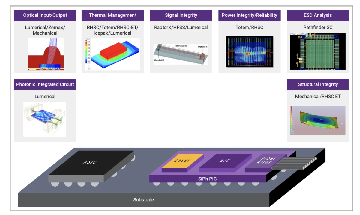

As global data traffic scales toward unprecedented heights, the semiconductor and networking industries are confronting a fundamental physical limitation in traditional hardware architectures. The rapid proliferation of artificial intelligence (AI), machine learning (ML), and high-performance computing (HPC) has pushed data center requirements from 400G and 800G toward the 1.6T (terabit) threshold. At these speeds, traditional electrical interconnects and pluggable optical modules are encountering severe bottlenecks related to power consumption, signal integrity, and physical reach. Co-packaged optics (CPO) has emerged as the critical architectural shift required to overcome these barriers, moving optical components directly onto the same package as the silicon switch or processor to drastically reduce electrical path lengths and enhance energy efficiency.
The Shift Toward Integrated Photonics
The fundamental driver behind the adoption of co-packaged optics is the diminishing return of traditional copper-based electrical signaling. In standard data center configurations, signals travel from a high-capacity switch ASIC (Application-Specific Integrated Circuit) through a printed circuit board (PCB) to a pluggable optical transceiver located at the front panel of the rack. As data rates increase, the "reach" or distance that an electrical signal can travel over copper without significant degradation shrinks. To compensate for this signal loss, engineers have historically relied on complex SerDes (Serializer/Deserializer) technology and retimers, which consume significant amounts of power.
Co-packaged optics disrupts this paradigm by integrating the optical engine within the same multi-die package as the ASIC. By reducing the distance between the silicon and the optical conversion point from centimeters to millimeters, CPO significantly lowers the "power per bit" metric. This proximity allows for the use of shorter-reach, lower-power electrical interfaces, effectively bypassing the signal integrity challenges inherent in long-reach copper traces.
Technical Drivers: Scaling to 800G and 1.6T
The transition to 800G and 1.6T networking represents a doubling and quadrupling of bandwidth that traditional pluggable form factors struggle to accommodate. In a typical 51.2 Tbps or 102.4 Tbps switch environment, the density of front-panel pluggable modules becomes a thermal and physical liability. The heat generated by dozens of high-speed transceivers packed into a single rack unit can exceed the cooling capacity of conventional air-cooled systems.
CPO addresses bandwidth density by leveraging silicon photonics to miniaturize optical components. By using advanced packaging techniques, such as 2.5D or 3.0D integration, manufacturers can place optical "tiles" or chiplets around the central processor. This configuration enables higher I/O (Input/Output) density than what is possible with edge-mounted pluggable modules. Furthermore, CPO facilitates the use of advanced modulation schemes like PAM4 (Pulse Amplitude Modulation 4-level) and coherent optics, which are essential for maintaining data integrity at 1.6T speeds over the longer distances required for inter-data center communication.

A Chronology of Interconnect Evolution
The evolution of data center interconnects has moved through several distinct phases, each defined by the balance between electrical and optical capabilities.
- The Discrete Era (Pre-2010): Networking relied heavily on discrete components and lower-speed copper cabling. Optical fiber was reserved for long-haul telecommunications, while data centers operated primarily on 1G and 10G electrical links.
- The Pluggable Revolution (2010–2020): The rise of SFP (Small Form-factor Pluggable) and later QSFP (Quad Small Form-factor Pluggable) modules allowed for modularity. Operators could swap modules to change distances or wavelengths. This era saw the jump from 40G to 100G and 400G.
- The Signal Integrity Crisis (2021–Present): As speeds reached 112G per lane, the electrical loss in PCBs became a primary design constraint. This period marked the beginning of intensive research into On-Board Optics (OBO) and the eventual development of CPO.
- The CPO Transition (2024 and Beyond): The industry is currently in the early adoption and standardization phase of CPO. Major hyperscalers and semiconductor giants are shifting from proof-of-concept to silicon-proven implementations, targeting 1.6T and 3.2T architectures.
Supporting Data and Performance Metrics
Recent industry benchmarks highlight the stark differences between traditional architectures and CPO-enabled designs. According to recent white papers and technical specifications released by Synopsys and industry consortiums, CPO can provide up to a 30% reduction in total power consumption for a 51.2T switch compared to pluggable optics.
Key data points include:
- Energy Efficiency: Traditional pluggable modules at 800G often consume approximately 15 to 20 picojoules per bit (pJ/bit). CPO aims to reduce this to under 5 pJ/bit by eliminating the need for power-hungry retimers and long-reach SerDes.
- Bandwidth Density: CPO enables an I/O density of over 1.5 Tbps per millimeter of die edge, a significant improvement over the physical constraints of front-panel ports.
- Latency Reduction: By moving the optical conversion closer to the compute engine, CPO reduces the propagation delay and signal processing latency, which is critical for real-time AI training clusters where microsecond delays can compound across thousands of nodes.
Multiphysics Challenges in CPO Design
Implementing co-packaged optics is not merely an exercise in shrinking components; it requires a sophisticated "multiphysics" approach to engineering. When optical components are placed in close proximity to high-power ASICs, several technical hurdles arise:
Thermal Management
The optical lasers and modulators used in CPO are highly sensitive to temperature fluctuations. However, the central ASIC in a high-end switch can generate hundreds of watts of heat. Managing this thermal gradient is essential. If the optical engine becomes too hot, its wavelength can shift, leading to signal loss or total link failure. Designers are increasingly turning to "External Laser Sources" (ELS) to keep the heat-generating laser away from the main package while keeping the modulators co-packaged.
Optical and Mechanical Alignment
Aligning a fiber optic cable to a silicon chiplet requires sub-micron precision. Unlike electrical pins, which can tolerate slight misalignments, optical paths must be perfectly coupled to avoid massive decibel (dB) losses. This necessitates advanced automated assembly processes and mechanical structures that can withstand the rigors of shipping and long-term operation in a data center environment.

Electrical Integrity
Even though the electrical paths are shorter in CPO, the high frequency of 112G and 224G signals means that crosstalk and electromagnetic interference (EMI) are still major concerns. Electronic Design Automation (EDA) tools must now simulate the electrical, thermal, and optical behaviors simultaneously to ensure the system functions as intended.
Official Responses and Industry Standardization
The move toward CPO is supported by a broad ecosystem of vendors and standards bodies. The Optical Internetworking Forum (OIF) has been instrumental in creating the "CPO Framework Implementation Agreement," which provides guidelines for the industry to ensure interoperability between different vendors’ components.
Leading semiconductor companies have voiced the necessity of this transition. Synopsys, a leader in EDA and IP solutions, has emphasized that silicon-proven interface IP is the backbone of CPO adoption. By providing pre-verified IP blocks for silicon photonics and high-speed SerDes, they enable chip designers to integrate optical capabilities without the risk of building custom solutions from scratch. Major cloud service providers (CSPs), including Google, Meta, and Microsoft, have also been vocal proponents, as their operational costs are directly tied to the power efficiency of their networking infrastructure.
Broader Impact and Implications for the AI Era
The implications of CPO extend far beyond simple networking. In the context of the current AI boom, CPO is viewed as an enabling technology for the next generation of "AI Factories." Modern AI models require massive clusters of GPUs or TPUs to be interconnected with low-latency, high-bandwidth fabrics. Traditional networking is increasingly seen as the "AI tax"—the overhead that limits the efficiency of these clusters.
By adopting CPO, data center operators can build larger, more efficient clusters that can train larger models in less time. Furthermore, the reduced power consumption of CPO contributes to the sustainability goals of major tech firms, who are under increasing pressure to mitigate the massive carbon footprint of their data centers.
Looking ahead, the success of co-packaged optics will depend on the continued maturation of the supply chain and the standardization of manufacturing processes. As 1.6T systems move toward high-volume production, CPO will likely transition from a niche high-end solution to the standard architecture for all high-performance interconnects. The integration of light and silicon represents the most significant shift in semiconductor packaging in decades, signaling an era where the boundaries between electronics and photonics are permanently blurred.
