

The global semiconductor landscape is undergoing a period of intense structural transformation, characterized by multi-billion dollar domestic investment surges, the standardization of emerging technologies, and a growing concern over the physical and human infrastructure required to sustain this growth. This week, the industry witnessed a confluence of strategic moves led by memory giant Micron and consumer electronics leader Apple, alongside critical warnings from trade organizations regarding a labor shortage that threatens to derail the ambitious fab construction schedules currently underway in the United States and abroad. As the sector pivots toward an AI-driven economy, the interplay between high-performance hardware, such as DDR5 and PCIe 6.0 storage, and the foundational standards for functional safety and connectivity has become the primary focus for engineers and policymakers alike.
Micron and Apple Lead Massive Domestic Investment Wave
Micron Technology has significantly accelerated its commitment to U.S.-based manufacturing, a move that aligns with the broader goals of the CHIPS and Science Act to reshore critical memory production. This week’s announcements highlight a multi-front expansion strategy. Micron’s investments are centered on two primary hubs: a state-of-the-art memory manufacturing facility in Boise, Idaho, and a massive "mega-fab" project in Clay, New York. These projects represent a long-term capital expenditure plan intended to ensure that the U.S. captures a significant share of the leading-edge DRAM market, which is increasingly vital for artificial intelligence applications.
Simultaneously, Apple has moved forward with a landmark $30 billion deal aimed at bolstering its domestic supply chain and engineering presence. While Apple has long been a major driver of semiconductor R&D through its custom silicon designs, this massive capital allocation signals a deeper integration with domestic manufacturing partners and specialized component providers. The investment is part of Apple’s broader five-year goal to contribute $430 billion to the U.S. economy, underscoring the shift toward "onshoring" critical technological capabilities to mitigate geopolitical risks and supply chain volatility.
Strategic Divestitures and the Evolving Packaging Market
The semiconductor ecosystem is also seeing a reshuffling of assets as companies narrow their focus to core competencies. Onsemi recently finalized the divestiture of certain non-core business units, a move that allows the power semiconductor specialist to concentrate more heavily on silicon carbide (SiC) and automotive power solutions. In tandem, Solstice’s recent acquisition activities indicate a consolidation trend in the niche materials and inspection segments.

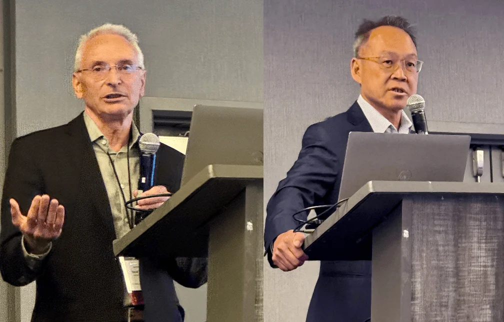
A significant point of discussion this week occurred at the iMAPS CHIPCon conference in Santa Clara, where executives from Amkor and ASE—the world’s leading Outsourced Semiconductor Assembly and Test (OSAT) providers—debated the future of advanced packaging. David McCann of Amkor and CP Hung of ASE highlighted that as Moore’s Law slows, the industry’s reliance on 2.5D and 3D packaging, as well as chiplet architectures, has transitioned from a luxury to a necessity. The primary challenge identified is the thermal management and interconnect density required for next-generation AI accelerators, which demand unprecedented levels of precision in wafer lapping and die-to-wafer bonding.
The Looming Workforce Crisis and Fab Construction Roadblocks
Despite the influx of capital, the semiconductor industry faces a "human capital" bottleneck that could prove more difficult to solve than any technical engineering hurdle. SEMI, the global industry association, issued a stark warning this week regarding the 189,000-worker shortage currently facing the sector. This deficit is not limited to high-level design engineers but extends to the skilled trades necessary to build and maintain the highly specialized environments required for chip production.
Large-scale fab projects require thousands of specialized workers, including pipefitters, electricians, and HVAC technicians trained in cleanroom protocols, safety, and contamination control. SEMI notes that the construction phase of these facilities is becoming a significant roadblock, as the demand for labor in regions like Arizona, Ohio, and Texas far outstrips the local supply. This shortage is expected to delay the "tool-in" dates for several major projects, potentially pushing back the timeline for domestic chip self-sufficiency.
In response to this crisis, educational institutions are ramping up their semiconductor portfolios. Purdue University, in collaboration with Taiwan’s National Yang Ming Chiao Tung University (NYCU), has expanded its professional education offerings to include joint courses in AI chip design and packaging. Meanwhile, New York’s Binghamton University recently opened a new cleanroom and microelectronic packaging research facility, aiming to train over 100 students annually to feed the burgeoning "Silicon Empire" in upstate New York. Furthermore, the Information Technology and Innovation Foundation (ITIF) has advocated for the creation of a new visa category for foreign technical experts, arguing that current U.S. immigration policy is a direct threat to industrial competitiveness.
Advancements in AI Infrastructure and Functional Safety
The technical side of the industry continues to move at a relentless pace, particularly in the realm of AI infrastructure. Rambus has introduced a new DDR5 server RDIMM chipset capable of operating at 9600 MT/s, a speed essential for the massive data throughput required by "agentic" AI and high-performance computing (HPC) clusters. Samsung Electronics has also entered mass production of its PCIe 6.0 SSDs, offering capacities ranging from 4TB to 16TB. These storage solutions are optimized for the heavy read/write cycles of AI training models, where data latency can be the difference between a successful model and a system crash.

As these chips become more powerful, the standards governing them must evolve. Accellera has released a draft version of its Functional Safety Language (FSL) standard. This is a critical development for the automotive and industrial sectors, as it provides a unified syntax for exchanging functional safety intent across different design tools. In an era where silicon failure can have life-or-death consequences in autonomous vehicles, the FSL standard aims to reduce the ambiguity that often leads to costly design errors.
Connectivity standards are also under the microscope. At recent industry events, experts highlighted the growing confusion surrounding USB and eUSB standards. While the new iterations offer higher bandwidth, the backward incompatibility and the sheer variety of "flavors" of USB4 have created integration headaches for system designers. Cadence’s David Shin pointed out that the industry must find a way to harmonize these standards to prevent a fragmented ecosystem that frustrates consumers and slows product adoption.
The Quantum Frontier: Chaos and Consolidation
Quantum computing remains the industry’s most experimental and volatile frontier. Experts describe the current state of the market as one where "maximum creativity meets maximum chaos." There is no consensus on which qubit technology—superconducting, trapped ion, or photonic—will ultimately prevail. This uncertainty has led to a proliferation of startups, followed by the inevitable wave of consolidation.
A major milestone was reached this week with IQM Quantum Computers becoming the first European quantum company to list on a major U.S. exchange following a SPAC deal. In a strategic move to bolster its software stack, IQM also acquired Quantistry, a firm specializing in AI-powered quantum chemistry simulations. This acquisition underscores the industry’s shift from building just the hardware to creating a full-stack solution that can solve real-world industrial problems, particularly in materials science and drug discovery.
Research Breakthroughs and New Technologies
University and corporate research teams continue to push the boundaries of materials science. A collaboration involving MITRE and UC Boulder has successfully built piezo-optomechanical photonic circuits directly on commercial CMOS driver wafers. This monolithic integration is a significant step toward creating dense electronic controls for silicon nitride photonics, which are essential for the next generation of sensors and quantum computers.

In the realm of transistor technology, researchers from San Jose State University and Sandia National Labs published a study on the radiation hardness of 3nm Gate-All-Around (GAA) FET-based SRAM. Their findings are crucial for the aerospace and defense industries, where chips must operate in the harsh, high-radiation environment of space. Additionally, Caltech has demonstrated a new chip that can redirect light beams in less than a trillionth of a second using the optical Kerr effect, a breakthrough that could revolutionize all-optical beam steering for LIDAR and high-speed communications.
Broader Impact and Industry Outlook
The semiconductor industry is currently navigating a period of "forced maturity." The transition from a globalized, just-in-time supply chain to a more localized, resilient model is proving to be both expensive and logistically daunting. While the $30 billion investments and 9600 MT/s chipsets capture the headlines, the success of the industry over the next decade will likely depend on the "unseen" infrastructure: the training of thousands of technicians, the standardization of safety languages, and the resolution of construction bottlenecks.
The data suggests that while the demand for silicon—driven by AI, EVs, and 5G—is insatiable, the industry’s ability to supply that silicon is currently constrained by the physical limits of human labor and the complexities of advanced manufacturing. As companies move toward the "Future of Memory and Storage" and "SEMICON Taiwan" later this year, the focus will remain squarely on how to bridge the gap between the ambitious investment goals of today and the operational realities of tomorrow. The industry is no longer just about designing the fastest chip; it is about building the ecosystem capable of producing it at scale.
