

The manufacturing of high-frequency, high-performance electronics relies heavily on the utilization of Liquid Crystal Polymer (LCP) as a substrate material. Renowned for its superior dielectric properties, thermal stability, and exceptional mechanical robustness, LCP has become the material of choice for the next generation of 5G infrastructure, automotive sensors, and advanced medical devices. However, the inherent chemical inertness of LCP poses a significant hurdle in the fabrication process: its extremely smooth surface and low surface energy make it notoriously difficult to plate with copper.

For years, the industry has relied on Potassium Hydroxide (KOH) chemical etching to achieve the necessary surface roughening required for electroless copper plating. While effective, this chemical-heavy approach introduces substantial operational and safety liabilities. As the electronics industry pivots toward more sustainable and streamlined manufacturing, the transition to plasma-based surface treatment has emerged as a critical technological inflection point. Recent findings from the applications team at Nordson Electronics Solutions, utilizing the Nordson MARCH MaxVIA system, provide a robust empirical case for why plasma processing is poised to replace traditional, chemistry-intensive methods.
The Industrial Challenge of LCP Metallization
Liquid crystal polymers are classified as thermoplastic polymers with a highly ordered, crystalline structure. While this structure grants LCP its remarkable thermal and electrical characteristics, it also renders the surface resistant to wetting. In a standard printed circuit board (PCB) manufacturing sequence, the inability to properly adhere copper to the LCP substrate leads to delamination, signal integrity loss, and premature component failure.

Historically, the industry addressed this through wet chemical processing. Potassium hydroxide (KOH) acts as a harsh etchant, chemically attacking the surface of the polymer to create microscopic anchor points for plating. This method, however, carries significant overhead. It requires specialized chemical handling, stringent environmental compliance measures for wastewater treatment, and dedicated facility space that many modern, agile PCB manufacturers simply do not possess. The industry has long sought an alternative that offers the same degree of mechanical interlocking without the corrosive risks associated with strong alkaline solutions.
A Chronology of Process Development
The shift toward plasma technology was not instantaneous but resulted from a deliberate, phased research and development effort. The objective was to prove that a dry, vacuum-based process could replicate the topography achieved by chemical etchants.

The evaluation process, conducted by the Nordson applications team, followed a rigorous three-step protocol designed to prepare the LCP surface for metallization:
- Cleaning and Pre-conditioning: The initial phase focused on removing organic contaminants and residues left behind from previous manufacturing stages.
- Surface Roughening (Etching): Utilizing a specialized gas chemistry, the plasma system was calibrated to etch the LCP surface at a controlled rate, creating the precise degree of roughness required for metal adhesion.
- Surface Activation: The final step involved a hydrogen and nitrogen (H2/N2) gas mixture, which functionalizes the surface, increasing its energy and ensuring that the electroless copper plating process can achieve uniform coverage.
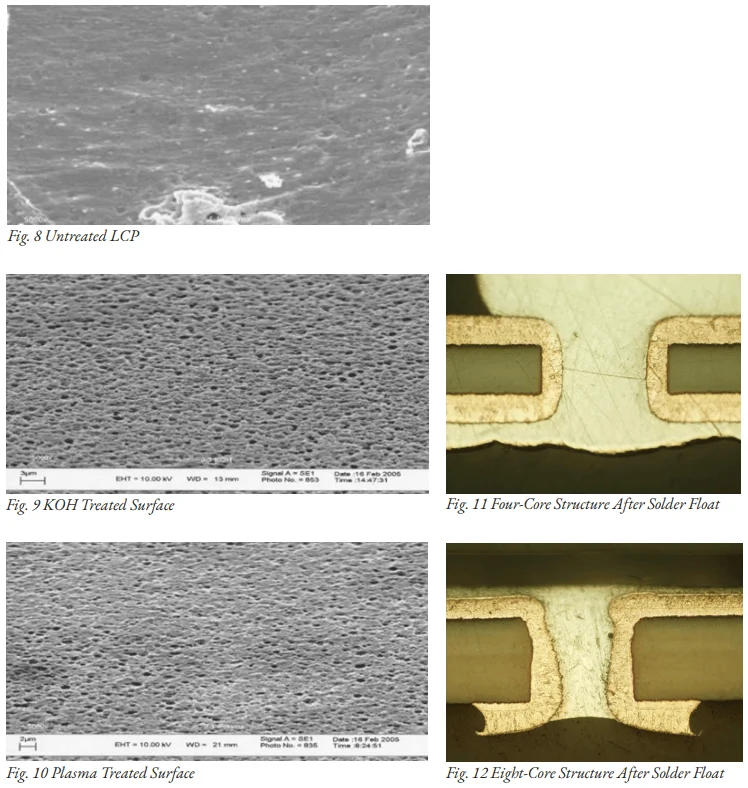
Following the initial testing phase, the team engaged in a series of comparative experiments to validate the efficacy of each step. Cross-sectional analysis and Scanning Electron Microscopy (SEM) were employed to inspect the topography of the treated substrates. The data confirmed that the plasma process did not merely strip the surface; it created a uniform, textured landscape that provided the ideal foundation for metallization.

Supporting Data and Technical Validation
The technical viability of this process was quantified through rigorous performance metrics. A key focus of the study was the necessity of the H2/N2 activation step. Researchers observed that while plasma etching successfully roughened the LCP, it was insufficient on its own to guarantee a high-quality, continuous copper layer. Without the activation step, the electroless copper plating exhibited gaps and poor adhesion. By integrating the activation phase, the team achieved full, uniform coverage, effectively demonstrating that the synergistic combination of physical etching and chemical activation is the critical success factor.
Further optimization testing focused on throughput efficiency. In industrial manufacturing, every minute counts toward the total cost of ownership. The team evaluated treatment durations of 20, 30, and 60 minutes. The data revealed that the process could be condensed to a 30-minute window without compromising the surface integrity or the subsequent plating quality. This reduction in cycle time directly translates to higher throughput in high-volume production environments, making plasma processing a competitive alternative to the traditional, time-consuming chemical baths.

Implications for PCB Manufacturing
The move toward plasma-based LCP treatment represents a broader trend in the electronics industry toward "dry" manufacturing. Beyond the safety benefits, the use of a system like the Nordson MARCH MaxVIA provides greater process control. Plasma processing is highly repeatable, governed by precise vacuum, power, and gas-flow parameters. Unlike chemical baths, which degrade over time as the concentration of reactants shifts, plasma systems offer a consistent environment where every board receives identical treatment.
Industry analysts suggest that the ability to adopt plasma processing for LCP will allow smaller and mid-sized PCB manufacturers to enter the high-frequency electronics market. By removing the need for a complex chemical infrastructure, manufacturers can integrate LCP handling into their existing lines with minimal modifications. This decentralization of high-performance manufacturing capability is expected to accelerate the development of 5G, automotive radar, and satellite communication components.

Expert Perspectives and Operational Reality
Kobe Zhang, an application supervisor at Nordson Electronics Solutions, has emphasized that the transition to plasma is driven by both technical necessity and operational efficiency. While the industry is inherently cautious about changing established workflows, the empirical evidence provided by modern plasma systems is difficult to ignore. The ability to perform "clean" processing—eliminating the risk of chemical splashes, toxic fumes, and the disposal of hazardous byproduct—aligns with the industry’s increasing focus on environmental, social, and governance (ESG) standards.
Furthermore, the solder float testing conducted during this project provides a vital assurance for original equipment manufacturers (OEMs). Solder float tests simulate the thermal stress that a PCB undergoes during assembly, exposing the board to molten solder temperatures. The fact that the plasma-treated LCP structures passed these tests on both four-core and eight-core configurations confirms that the adhesion is not just a surface-level phenomenon but a robust, thermally stable bond capable of surviving the rigors of modern manufacturing.

The Broader Impact
As the demand for LCP-based components grows, the industry’s reliance on antiquated chemical methods poses a bottleneck to production. The successful optimization of plasma processing marks a departure from reliance on dangerous, high-maintenance chemical infrastructure toward a precision-engineered, scalable, and environmentally conscious alternative.
The implications for the supply chain are significant. With the ability to reliably process LCP, manufacturers can leverage the unique properties of the material to design smaller, faster, and more efficient electronics. The research performed by the Nordson team serves as a roadmap for this transition, providing the necessary data to justify the transition to plasma-based technology. As high-speed data transmission becomes the backbone of the global economy, the underlying manufacturing processes—such as this optimized approach to LCP surface activation—will prove to be the unsung heroes of the next technological revolution.

In summary, the transition from KOH-based etching to plasma processing for LCP is not merely a matter of convenience; it is a critical optimization of the manufacturing workflow. By delivering consistent, high-performance results through a cleaner, more efficient, and more controllable process, plasma technology has secured its place as the industry standard for the future of electronics fabrication. Through rigorous testing and data-driven process development, the industry has successfully unlocked the full potential of LCP, clearing the path for the next generation of high-frequency hardware.
