
The Architectural Bottleneck of LLM Decoding
The fundamental challenge in LLM inference lies in the decoding phase. Unlike the "prefill" phase, where an entire prompt is processed in parallel with high arithmetic intensity, the decoding phase generates tokens one by one. Each new token requires the entire set of model weights to be fetched from memory, yet performs relatively few calculations per byte of data retrieved. This results in a low arithmetic intensity, making the performance of LLM decoding almost entirely dependent on memory bandwidth rather than raw compute power.
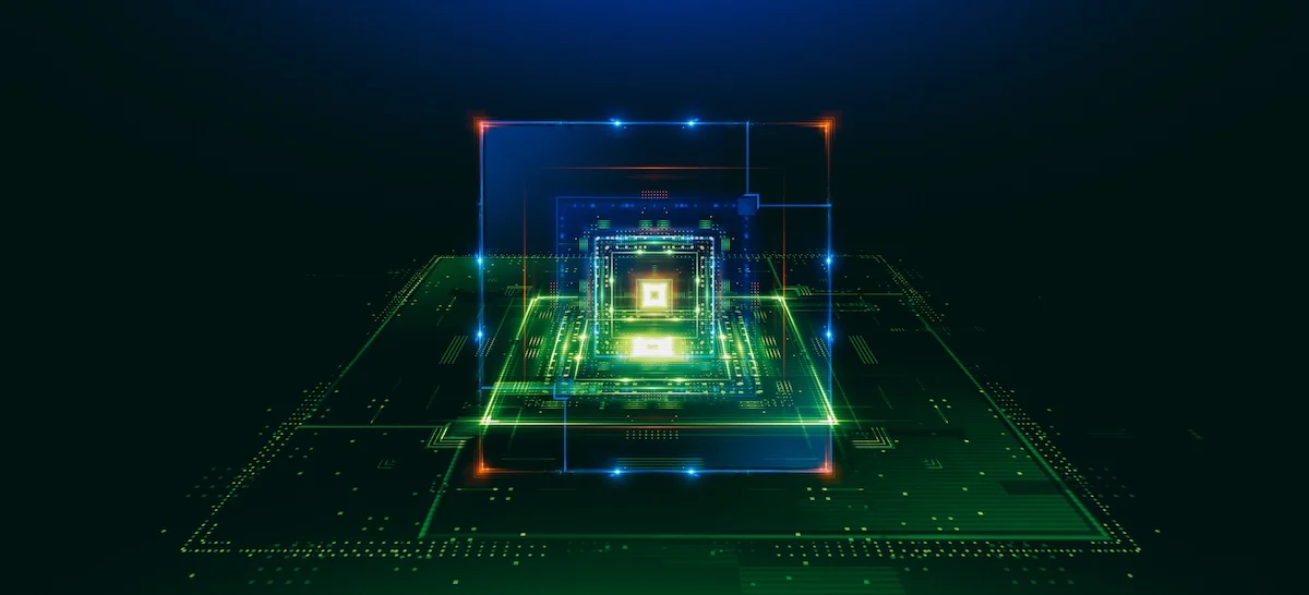
Conventional hardware, including state-of-the-art GPUs, relies on off-chip memory interfaces such as High Bandwidth Memory (HBM). While HBM offers significant throughput, the physical distance and the energy cost of moving data across the bus create a "memory wall." 3D-stacked Near-Memory Processing (NMP) has emerged as a potential solution. In an NMP configuration, a logic die is integrated directly beneath or within a stack of DRAM layers (such as HBM or Hybrid Memory Cube). This proximity allows for massive internal bandwidth and reduced latency, theoretically solving the data movement issue.
However, the researchers behind "Rethinking Compute Substrates" identified a critical secondary problem: when the memory bandwidth bottleneck is removed by NMP, the system immediately encounters a compute bottleneck. Because the logic die in a 3D stack is severely limited by area and thermal constraints, it cannot simply house a massive array of standard processors. The study reveals that prior NMP designs, which utilized basic Multiply-Accumulate (MAC) tree-based compute units, are insufficient for the diverse shapes and operators found in modern LLM workloads.
The Shift to Reconfigurable Systolic Arrays
A core contribution of the paper is the transition from MAC tree-based units to a more area-efficient systolic array microarchitecture. In a systolic array, data flows through a grid of processing elements (PEs) in a rhythmic fashion, reducing the need for constant access to global registers or caches. This design is highly efficient for matrix multiplications, which constitute the bulk of LLM workloads.
The researchers observed that LLM decoding operators exhibit "substantial shape diversity." Depending on the specific layer of the transformer model or the size of the attention head, the dimensions of the tensors being processed can vary significantly. To address this, the proposed microarchitecture features fine-grained reconfigurability in both the shape of the systolic array and the dataflow patterns it supports. This flexibility ensures that the compute substrate maintains high utilization regardless of the specific mathematical operation being performed.
Furthermore, the team exploited a unique opportunity provided by the 3D-stacked environment. Because the local memory bandwidth is so high, the need for large, area-consuming on-chip buffers is diminished. The researchers were able to unify the systolic array with existing vector cores—originally intended for auxiliary tasks like activation functions or layer normalization. By sharing control logic and multi-ported buffering between the vector core and the systolic array, the design achieves a highly compact footprint suitable for the tight area budget of a 3D-stacked logic die.
Chronology of NMP Development and LLM Optimization
The publication of this research in April 2026 marks a decade-long evolution in near-memory processing. The timeline of this technological progression highlights the urgency of the "Rethinking Compute Substrates" paper:
- 2013–2015: The introduction of the Hybrid Memory Cube (HMC) and High Bandwidth Memory (HBM) standards established the physical foundation for 3D stacking.
- 2018–2021: Early NMP research focused on simple database acceleration and basic vector operations. Projects like "Tesseract" explored NMP for graph processing, but LLMs were not yet the primary focus.
- 2023: The "Generative AI Boom" created a crisis in data center energy consumption. Hardware designers began prioritizing "Memory-Centric" architectures over "Compute-Centric" ones.
- 2024: The "Stratum" design emerged as a leading benchmark for 3D-stacked NMP, using MAC-tree architectures to improve LLM throughput.
- 2025: Industry leaders like TSMC and Samsung announced advanced 3D packaging technologies (CoWoS and X-Cube) capable of supporting more complex logic dies within memory stacks.
- April 2026: The University of Edinburgh and its partners published the current paper, identifying the limitations of Stratum and proposing the microarchitecture-scheduling co-design that defines the next generation of NMP.
Supporting Data and Performance Benchmarks
The research team conducted extensive simulations to compare their proposed microarchitecture against "Stratum," the previous gold standard for NMP LLM acceleration. The evaluation covered both "Dense" models (where every parameter is active for every token) and "Mixture-of-Experts" (MoE) models (where only a subset of parameters is activated).
The results demonstrated a significant leap in performance:

- Speedup: The proposed design achieved an average 2.91x speedup in decoding latency compared to Stratum.
- Energy Efficiency: The architecture provided 2.40x higher energy efficiency, measured in performance per watt.
- Area Efficiency: By unifying the vector core and systolic array, the design stayed within the 3D logic die’s strict area constraints while outperforming larger, more traditional designs.
- Utilization: The reconfigurable dataflow allowed the systolic array to maintain over 80% utilization across various tensor shapes, a significant improvement over the static MAC-tree approach.
The inclusion of MoE models in the testing is particularly noteworthy. MoE architectures, such as those used in the GPT-4 class of models, are notoriously difficult for hardware because they involve sparse, unpredictable memory access patterns. The fine-grained reconfigurability of the proposed NMP substrate proved especially effective at handling the dynamic nature of MoE decoding.
Industry Implications and Expert Analysis
While the paper is a technical academic contribution, its implications for the semiconductor and cloud computing industries are profound. As the "arms race" for AI supremacy continues, the ability to serve LLM requests faster and with lower power costs is a massive competitive advantage.
Industry analysts suggest that this research could influence the roadmap for next-generation AI accelerators. Companies like NVIDIA, AMD, and Tenstorrent are increasingly looking toward 3D integration to solve the bandwidth problem. The "Rethinking Compute Substrates" paper provides a blueprint for how these companies might design the logic layer of their future 3D-stacked chips.
"The shift from being memory-bound to compute-bound within the NMP environment is a nuance that many early designs missed," noted an industry consultant specializing in AI hardware. "By identifying that the logic die itself is the new bottleneck, this research team has pivoted the conversation toward microarchitectural efficiency rather than just raw bandwidth."
Furthermore, the multi-core scheduling framework proposed in the paper addresses the "orchestration" problem. In a 3D-stacked environment, managing multiple compute cores across different memory layers requires sophisticated scheduling to avoid thermal hotspots and ensure data remains local to the processing units. The proposed framework ensures that the high-bandwidth potential of the 3D stack is not wasted by idle cores or inefficient task distribution.
Broader Impact and Future Directions
The success of this microarchitecture-scheduling co-design signals a broader shift in computer science toward "Domain-Specific Architectures" (DSAs). As general-purpose CPUs and GPUs reach the limits of Moore’s Law, specialized hardware tailored for specific algorithms—like transformer-based LLMs—becomes essential.
The environmental impact is also a key consideration. Data centers currently consume a significant percentage of global electricity, much of it driven by AI inference. A 2.4x improvement in energy efficiency, if implemented at scale, could result in a massive reduction in the carbon footprint of global AI operations.
Looking ahead, the researchers suggest that the next step is the physical prototyping of the reconfigurable systolic NMP die. While the current results are based on high-fidelity architectural simulations, the move to silicon will require addressing the thermal challenges of stacking high-performance logic directly beneath heat-sensitive DRAM.
In conclusion, "Rethinking Compute Substrates for 3D-Stacked Near-Memory LLM Decoding: Microarchitecture-Scheduling Co-Design" represents a critical milestone in AI hardware research. By solving the dual challenges of memory bandwidth and compute utilization through an innovative, area-efficient design, the collaborative team has provided a scalable solution for the future of large-scale language model deployment. As the industry moves toward 2027 and beyond, the principles laid out in this study are likely to become foundational to the next generation of AI silicon.
