
The semiconductor industry is currently undergoing a fundamental transformation in how system components communicate, driven by the insatiable data demands of artificial intelligence and the architectural shift toward heterogeneous integration. As chips grow increasingly complex and packaging options like 2.5D and 3D stacking become mainstream, designers are no longer simply choosing a wire; they are architecting sophisticated communication fabrics that span from the microscopic pathways within a die to the fiber-optic cables connecting massive server racks. Fast and efficient data flow has become the primary metric of success, particularly in AI systems where the volume of information moving between processors and memory is staggering. If data cannot reach the processor fast enough, the resulting latency creates bottlenecks that negate the performance gains of the most advanced silicon. This shift has elevated interconnect selection from a peripheral design task to a central, system-level implementation decision that dictates the thermal, electrical, and economic viability of modern computing hardware.
The Evolution of Connectivity: From Monolithic to Modular
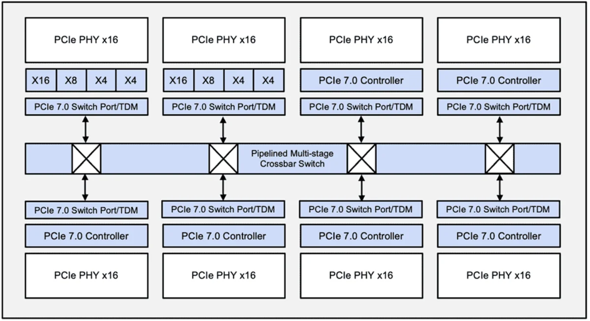
Historically, system connectivity was a relatively straightforward choice between a few established standards like PCI Express (PCIe) for board-level components and Ethernet for networking. However, the slowing of Moore’s Law has forced the industry toward "disaggregation"—breaking large, monolithic chips into smaller, specialized "chiplets." This modular approach allows manufacturers to mix and match different process nodes and functions, but it introduces a massive challenge: how to connect these pieces without losing speed or consuming excessive power.
The timeline of this evolution shows a clear trajectory toward standardization. Five years ago, architects typically selected a single interconnect and a single package for a design. Today, a single AI accelerator might simultaneously employ Universal Chiplet Interconnect Express (UCIe) for die-to-die links, Compute Express Link (CXL) for memory pooling, and proprietary or emerging standards like UALink for GPU-to-GPU scaling. This "layered approach" reflects a maturing industry that recognizes no single protocol can meet every requirement for bandwidth, latency, and distance.
Decoding the Terminology: I/O versus Interconnect
A critical distinction has emerged in the industry between "I/O" and "interconnect," terms that were once used interchangeably. According to industry experts, including Priyank Shukla of Synopsys, "interconnect" refers to the physical layer that connects chips or dies, such as PCIe or UALink. In contrast, "I/O" (Input/Output) is increasingly viewed as the general-purpose, lower-speed physical interface that lacks the specialized controllers found in high-speed interconnects.

Furthermore, the rise of I/O chiplets—dedicated dies that handle data movement for a core compute die—has changed the physical landscape of the package. These components must manage signal degradation and thermal hotspots, which are common when pushing massive amounts of data through narrow pathways. Designers must now weigh options across interface protocols, physical buffer designs, and intricate wiring pathways for both on-chip and off-chip networks, ensuring that the "plumbing" of the system does not become its weakest link.
The Chiplet Revolution and the Rise of UCIe
Among the most significant developments in recent years is the industry-wide push for standardized chiplet interfaces. For years, companies like AMD and Intel used proprietary die-to-die links, creating "vendor lock-in" that prevented the mixing of components from different manufacturers. The introduction of UCIe (Universal Chiplet Interconnect Express) aims to solve this by providing a standardized stack and compliance testing framework.
Mick Posner of Cadence notes that while PCIe is the "gold standard" for board-level connectivity, the industry is still searching for a "PCIe of die-to-die." UCIe is the leading candidate to fill this role, offering the promise of an open ecosystem where a designer could, in theory, buy a processor chiplet from one vendor and an I/O chiplet from another, plugging them into the same package. This interoperability is expected to drastically reduce verification burdens and ecosystem friction, though the complexity of implementing these multi-vendor stacks remains a significant hurdle for engineering teams.
The High-Stakes Battle for AI Data Center Dominance
In the data center, the competition for interconnect dominance is fierce, particularly regarding "scale-up" (connecting processors within a rack) and "scale-out" (connecting racks across a facility). Currently, NVIDIA’s proprietary NVLink leads the market for GPU-to-GPU communication, offering ultra-high bandwidth tailored specifically for AI workloads. However, a coalition of competitors including AMD, Broadcom, and Intel has introduced UALink (Ultra Accelerator Link) as an open-standard alternative.
The choice between these standards involves more than just technical specifications; it is a strategic "hedging of bets." As Saurabh Gayen of Baya Systems points out, technology does not always win based on technical superiority alone—momentum and ecosystem support are often more decisive. While UALink is built from the ground up for AI-specific needs, Ethernet remains a formidable incumbent. Initiatives like the Ultra Ethernet Consortium and ESUN (Ethernet for Scale-Up Networking) seek to tweak existing Ethernet infrastructure to handle AI traffic, leveraging the comfort and expertise hyperscalers already have with the protocol.

Memory Bottlenecks and the Role of CXL
The "memory wall"—the gap between how fast a processor can compute and how fast it can access data—remains a primary concern for AI architects. Compute Express Link (CXL) has emerged as a vital tool for addressing this, enabling memory sharing and pooling. Unlike traditional protocols, CXL allows multiple compute nodes to dynamically access a shared pool of memory, improving utilization and reducing the need for expensive, redundant storage.
As AI models grow to trillions of parameters, the ability to move data efficiently between CPUs, GPUs, and High Bandwidth Memory (HBM) is paramount. CXL 3.1 and future iterations are expected to pull more of the accelerator attach story toward coherent fabrics, which is essential for workloads where data movement is the primary performance constraint rather than raw mathematical operations.
The Hidden Cost of Proliferation: Bugs and Validation
While the abundance of interconnect options provides designers with more choices, it also introduces unprecedented risks. Ashish Darbari, CEO of Axiomise, warns that the "proliferation itself is part of the problem." When an architect "stitches together" a stack of different protocols—such as UCIe for compute, PCIe for I/O, and specialized NoCs (Networks on Chip) for accelerators—bugs are likely to emerge in the "seams" between these different layers.
No single entity owns the entire stack in these complex multi-die systems, making verification a monumental task. Every custom or proprietary link adds a "permanent tax" on validation and supply-chain optionality. This has led to a growing preference for "boring" standardization among engineers, as the cost of a failed interconnect strategy can be catastrophic, potentially rendering an entire product line obsolete before it even hits the market.
The Future is Optical: The Shift to Co-Packaged Optics
As electrical interconnects reach their physical limits in terms of bandwidth and power efficiency, the industry is looking toward light. Many experts predict that within the next five years, a significant portion of AI data center interconnects will transition to optical technology. TrendForce data supports this trend, predicting that the global shipment of optical transceivers will triple from 26.5 million units in 2023 to over 92 million units by 2026.

Co-packaged optics (CPO) and silicon photonics represent the next frontier. By integrating optical components directly into the chip package, designers can overcome the signal loss and thermal limits associated with copper wiring. Optical I/O offers the promise of moving data over longer distances with much lower power consumption, though it currently remains a niche solution due to high manufacturing costs and technical complexity. However, as AI chips become increasingly "bandwidth-hungry," the move from electrical to optical signaling is becoming an inevitability rather than a choice.
Conclusion: A Multi-Fabric Reality
The semiconductor landscape is unlikely to be governed by a single, "winner-take-all" interconnect standard. Instead, the industry is settling into a nuanced, multi-fabric reality where different protocols serve specific niches. PCIe will likely remain the default for broad compatibility; CXL will dominate memory semantics and pooling; UCIe will lead the chiplet revolution; and specialized links like NVLink and UALink will battle for high-speed accelerator domains.
The systems that succeed in this new era will be those that blend these various links cleanly, managing the "seams" between protocols with sophisticated software and robust verification. For designers, the challenge is no longer just building a faster processor, but building a more cohesive network. In the world of AI-driven computing, the strength of the system is entirely dependent on the speed and reliability of the connections that hold it together. As the economics of data centers shift and the technical hurdles of copper wiring mount, the innovations in interconnect technology will remain the most critical factor in the ongoing evolution of high-performance silicon.
