

As the semiconductor industry pushes toward the 2-nanometer (nm) node and beyond, the traditional methods of delivering power to transistors have reached a critical bottleneck. For decades, both signal and power were routed through the front side of the wafer in the Back-End-of-Line (BEOL) layers. However, as transistors shrink, the metal layers on the front side have become increasingly congested, leading to significant voltage drops (IR drop) and a reduction in overall chip performance. To circumvent these physical limitations, the industry is transitioning toward Backside Power Delivery Networks (BSPDNs), a revolutionary architectural shift that decouples power delivery from signal routing. This transition requires the integration of advanced features such as buried power rails (BPRs) and nano-through-silicon vias (nTSVs). A recent collaborative study between the Semiverse Solutions team at Coventor (a Lam Research Company) and imec has utilized advanced predictive modeling to address the complex integration challenges associated with these structures, specifically focusing on the impact of overlay and patterning effects on electrical resistance.
The Architectural Evolution: From Frontside to Backside Power Delivery
The fundamental problem addressed by BSPDNs is one of physical congestion. In a traditional chip architecture, all power and signal wiring compete for space in the metal layers above the transistors. This is often compared to a crowded office building where employees, visitors, and delivery services all share a single front entrance. As the volume of traffic increases, the hallway becomes a bottleneck, slowing everyone down. In semiconductor terms, this congestion increases the resistance of the power lines, leading to heat generation and power inefficiency.
By moving the power delivery network to the backside of the wafer, engineers effectively create a "back hallway" dedicated solely to power. This leaves the front side of the chip—the traditional BEOL—free to handle signal routing with less interference. This separation allows for thicker, lower-resistance power lines on the backside, which significantly reduces the IR drop and improves the power-performance-area (PPA) metrics of the device. However, connecting this backside network to the transistors on the front side requires drilling through the silicon substrate using nTSVs, which must land precisely on BPRs embedded deep within the device architecture.

Technical Foundations: nTSVs and Buried Power Rails
The implementation of a BSPDN relies on two critical "scaling boosters": Buried Power Rails (BPRs) and nano-Through-Silicon Vias (nTSVs). BPRs are metal lines buried within the transistor’s STI (Shallow Trench Isolation) or below the device level, acting as local power distribution hubs. Because they are situated lower in the stack than traditional power rails, they provide more space for signal routing above.
The nTSVs serve as the vertical electrical bridge between the BPR and the backside of the wafer. These vias are significantly smaller than traditional TSVs used in 3D packaging, often measuring only a few dozen nanometers in diameter. The integration process is delicate: the wafer must be thinned from the backside to expose the silicon, and then nTSVs are etched and filled to create the connection. The success of this architecture depends entirely on the quality of the electrical contact between the nTSV and the BPR. If the connection is misaligned or if the shape of the via is distorted during patterning, the resistance increases, potentially negating the benefits of the BSPDN or causing total device failure.
The Collaborative Research Context: The ID2PPAC Project
The analysis conducted by the Semiverse Solutions team and imec was performed under the umbrella of the ID2PPAC project. This joint undertaking, supported by imec and the Electronic Components and Systems for European Leadership (ECSEL) program, is a strategic initiative aimed at ensuring European leadership in the next generation of logic technology. The primary objective of the ID2PPAC project is to demonstrate that the demanding performance, power, area, and cost (PPAC) requirements of the 2-nm node can be met through innovative system-scaling boosters.
As part of this research, the teams focused on the nTSV-to-BPR connection, which is widely considered one of the most difficult integration points in the BSPDN flow. To optimize this connection without the prohibitive cost and time of physical wafer fabrication, the researchers turned to virtual fabrication using SEMulator3D, a 3D process modeling platform.

Modeling the nTSV-BPR Connection Resistance
To accurately quantify the performance of the nTSV-BPR interface, the team utilized a virtual Cross-bridge Kelvin Resistor (CBKR) structure. In electrical engineering, a Kelvin measurement is a four-terminal sensing technique that allows for the measurement of very low resistances by isolating the resistance of the contact itself from the resistance of the surrounding metal lines.
Using SEMulator3D, the researchers simulated a full process step sequence to mirror realistic manufacturing conditions. This included lithography, etching, deposition, and chemical-mechanical planarization (CMP). By simulating the entire flow, the model could capture "non-ideal" geometric effects—such as the tapering of the via walls or the specific topography of the BPR—that are often missed in idealized CAD models.
The simulation results were benchmarked against Transmission Electron Microscopy (TEM) cross-sections of physical test chips. The virtual models showed a high degree of correlation with the actual physical profiles, confirming that the simulation could reliably predict the shape and volume of the nTSV-BPR junction.
Analyzing the Impact of Patterning and Overlay Effects
The study identified two primary factors that influence connection resistance: patterning effects (specifically corner rounding) and overlay (alignment) errors.

The Corner Rounding Effect
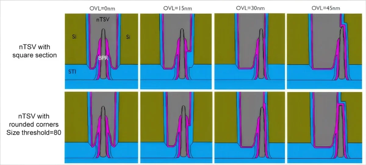
In nanoscale lithography, it is nearly impossible to maintain perfectly square corners for small features. Due to the physics of light diffraction and the chemical properties of photoresists, square-designed vias often result in rounded or circular profiles on the actual wafer. The research team compared idealized square nTSV profiles with process-realistic rounded-corner profiles.
The simulations revealed that rounded corners significantly decrease the total contact area between the nTSV and the BPR. Because resistance is inversely proportional to the contact area, this rounding effect inherently increases the resistance. More importantly, the simulation showed that rounded corners make the connection much more sensitive to any misalignment.
The Overlay Sensitivity
Overlay refers to the precision with which the nTSV is aligned with the BPR. If the nTSV is shifted even a few nanometers to the side, the overlap area decreases. The study performed a "sweep" of overlay dimensions from 0 nm (perfect alignment) to 45 nm (significant misalignment).
The findings were definitive:

- The 30nm Safety Threshold: To guarantee a functional connection between the nTSV and the BPR, the overlay error must be kept under 30 nm. Beyond this point, the contact area becomes so small that resistance spikes exponentially, leading to poor chip performance.
- The 15nm Optimal Window: For high-yield manufacturing and optimal power delivery, the simulation indicated that the overlay should be limited to approximately 15 nm. Within this window, the resistance remains low and stable, providing the tight control necessary for 2-nm node logic.
Supporting Data and Simulation Highlights
The virtual electrical simulations provided a predictive model that mimicked the minimum values found in actual physical measurement distributions. This validation is crucial for semiconductor manufacturers, as it allows them to define "process windows"—the range of manufacturing tolerances within which a chip will still function correctly.
Data from the SEMulator3D analysis showed that when patterning rounding was included in the model, the sensitivity to Edge Placement Error (EPE) increased by nearly 40% compared to idealized models. This highlights the danger of using overly simplified simulations during the design phase of advanced technology nodes. The predictive model also allowed the team to explore BPR contact area optimization, suggesting that slightly widening the BPR could provide a greater margin for overlay error, though this must be balanced against the overall goal of reducing the chip’s footprint.
Broader Industry Implications and Future Outlook
The move to Backside Power Delivery is not merely a theoretical exercise; it is a competitive necessity. Major industry players, including Intel, TSMC, and Samsung, have all announced roadmaps that include some form of BSPDN. Intel’s "PowerVia" technology is expected to be a cornerstone of its future nodes, while TSMC has introduced its "A16" process which will utilize backside power delivery to maintain its lead in the foundry market.
The research conducted by imec and the Semiverse Solutions team provides a roadmap for the rest of the industry. By demonstrating that predictive simulation can accurately model the resistance of nTSV-BPR connections, they have provided a tool that can significantly accelerate the development cycle. Instead of running hundreds of physical wafers to find the optimal alignment tolerances, engineers can use virtual fabrication to narrow down the parameters, saving millions of dollars in R&D costs.

Furthermore, as BPR dimensions continue to scale down below the 2-nm node, the margins for error will shrink even further. The ability to simulate the impact of process variations—such as etch depth variability or metal fill voids—will be essential for maintaining high yields in mass production.
Conclusion: The Role of Predictive Modeling in Yield Enhancement
The transition to BSPDN represents one of the most significant changes in semiconductor architecture in decades. While the benefits of reduced IR drop and increased routing density are clear, the integration challenges are formidable. The study titled "Optimizing Nano-TSV to BPR Connections for Backside Power Delivery Networks via Predictive Simulation" underscores the necessity of moving beyond idealized designs.
By incorporating realistic process effects like corner rounding and overlay error into 3D models, the Semiverse Solutions and imec teams have established a high-fidelity method for predicting electrical performance. Their findings—specifically the identification of the 15nm and 30nm overlay thresholds—provide critical guidance for the development of the 2-nm node. As the industry moves toward 1-nm and "Angstrom-era" devices, such predictive modeling will remain a cornerstone of semiconductor innovation, enabling the continued scaling of power and performance in an increasingly crowded physical landscape.
