

As the semiconductor industry pushes past the 2nm threshold, the traditional manufacturing silos that have defined silicon production for decades are rapidly disintegrating. At these extreme dimensions, the margin for error has effectively vanished. Transistor architectures are no longer just shrinking; they are becoming hypersensitive to environmental factors, material inconsistencies, and the mechanical stresses of advanced packaging. The transition to sub-2nm manufacturing represents one of the most significant engineering challenges in the history of the industry, as a single atomic displacement can now determine the difference between a high-performance processor and a scrap silicon wafer.
The Physics of Fragility and the End of Traditional Margins
Historically, chip manufacturing relied on generous safety margins. If a process deviated slightly, the physical bulk of the transistors and the thickness of the substrates provided enough structural stability to maintain functional integrity. That era has concluded. At sub-2nm nodes, the industry is dealing with geometries so small that quantum effects and atomic-level imperfections dominate the performance profile.
When wafers are thinned to accommodate the vertical stacking required for modern AI accelerators and high-performance computing (HPC) chips, they become exceptionally fragile. Standard wafer probing—the process of physically contacting a die with needles to test its electrical integrity—has become a liability. The pressure from these probes can easily damage delicate oxide layers or microscopic vias. Furthermore, as manufacturers move toward hybrid bonding—a technique essential for high-bandwidth, 3D-integrated circuits—the mechanical risks increase exponentially. There is no viable way to probe a hybrid bond without compromising the structural or electrical integrity of the connection. Consequently, manufacturers are increasingly forced to move to "known-good-die" testing methodologies or adopt sacrificial pad structures that are discarded before final assembly.
A Chronology of Increasing Complexity
The industry’s path to this point can be viewed through a decade-long transition in design priorities. In the 2010s, the focus was primarily on "scaling for power," where engineers simply sought to shrink features to reduce energy consumption. By 2018, the industry shifted toward "scaling for density," introducing FinFETs and early multi-die concepts.
The year 2024 marked a turning point, with the mass adoption of chiplet-based architectures. As the demand for raw processing power began to outstrip the physical limits of reticle-sized silicon dies, manufacturers turned to disaggregated designs. This, however, created a new set of logistical nightmares: thermal density and structural stress. A chiplet that operates perfectly in isolation may fail when integrated into a 3D stack due to the heat generated by its neighbors. This transition has forced the industry to reconsider redundant design architectures—a concept that was once the domain of 1990s-era mainframes but has now returned to the forefront of modern data center design to handle the inevitable manufacturing faults inherent in complex 3D assemblies.
The Challenge of Data Noise and False Positives
Perhaps the most insidious challenge for modern fabs is the explosion of "nuisance defects." As inspection equipment becomes more sensitive to capture sub-nanometer anomalies, it often fails to distinguish between a critical, functional-ending defect and a benign process variation. Prasad Bachiraju, senior director of business development at Onto Innovation, notes that current toolsets are capturing millions of defects, many of which are simply the result of process "noise" or normal neighborhood variations.

This phenomenon creates a signal-to-noise ratio crisis. If a fab engineer treats every detected anomaly as a potential failure, production grinds to a halt. If they ignore them, yield rates plummet. The industry is moving away from relying on inspection signals alone to decide what constitutes a "defective" part. Instead, companies like proteanTecs are advocating for the use of on-chip "agents"—embedded sensors that monitor the health of logic paths in real-time. By observing how actual logic behaves under stress, rather than simply measuring the physical dimensions of a feature, engineers can differentiate between harmless variations and conditions that will lead to premature field failure.
Integrating the Digital and Physical Supply Chain
The complexity of sub-2nm manufacturing has necessitated a move toward "virtualized" development. Lam Research’s Chief AI Officer, David Fried, emphasizes that the industry can no longer rely on the iterative, hardware-heavy R&D cycles of the past. There are simply too many process variables—often numbering in the hundreds—to map out through physical experimentation alone. Virtualization and predictive modeling are no longer optional; they are the primary tools for determining whether a process design will be robust enough for mass production.
This digital-first approach extends into the "orchestration layer," as described by PDF Solutions CEO John Kibarian. The goal is to create a seamless data loop that connects Product Lifecycle Management (PLM), Enterprise Resource Planning (ERP), and Manufacturing Execution Systems (MES). By removing the human element from the loop and allowing AI to make real-time decisions based on integrated data, fabs aim to manage the massive influx of information that would otherwise overwhelm traditional cloud-based analysis.
Implications for Future Reliability
The shift toward redundant server clusters and hierarchical test servers on individual dies signifies a fundamental change in how we define reliability. It is no longer enough to build a perfect chip; the industry must now build chips that are "aware" of their own health and capable of being repaired or bypassed if a fault occurs.
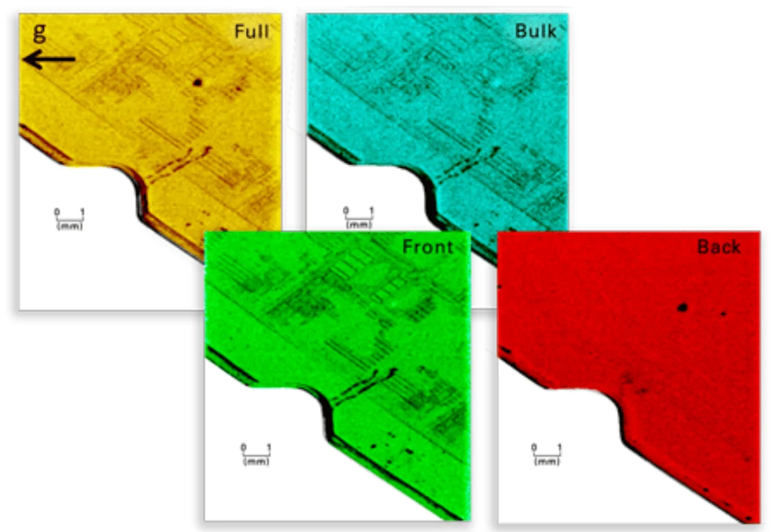
The use of X-ray tomography has become a critical tool in this effort, allowing engineers to look inside the chip at each stage of the manufacturing process to detect microfractures caused by warpage. This is particularly vital for the high-precision requirements of current-generation processors, where the metrology specifications must be held within the sub-angstrom range. If a front-end process introduces an error, it is amplified as the chip moves through the multi-die assembly chain. Detecting that error early, rather than at the end of a multi-billion-dollar packaging process, is now the primary driver of profitability in the semiconductor sector.
A New Era of Holistic Manufacturing
Ultimately, the challenges of the sub-2nm era have destroyed the concept of the "stand-alone" manufacturing step. Every action taken during the photolithography, etching, or deposition phase must now be evaluated for its downstream impact on thermal management, mechanical stability, and electrical timing. The lines between design, manufacturing, and testing have blurred into a single, continuous stream of information.
As the industry advances, the winners will be those who can best manage this complexity through hierarchical coordination. The future of silicon is not found in a single, perfect transistor, but in the sophisticated management of billions of components that are individually imperfect but collectively reliable. The transition to this holistic, data-driven manufacturing model is not merely an improvement on past practices; it is the prerequisite for the continued existence of Moore’s Law in an era where the laws of physics are increasingly pushing back. By embracing advanced metrology, on-chip diagnostic agents, and AI-driven orchestration, the semiconductor industry is attempting to turn the noise of sub-nanometer manufacturing into the signal of a new, highly resilient technological age.
