
A global consortium of researchers, spearheaded by Intel and representing a coalition of industry leaders, academic institutions, and national laboratories, has released a seminal perspective in the March 2026 issue of Nature Reviews Electrical Engineering, asserting that the future of global computing hinges on the strategic advancement of heterogeneous integration (HI). This architecture-level shift, which involves the sophisticated assembly of separately manufactured silicon components into a unified system-in-package, is no longer a luxury but a fundamental necessity for the continued progression of artificial intelligence (AI), 6G telecommunications, and high-performance autonomous systems. The researchers warn that while the physical capabilities of advanced packaging have surged over the last decade, the strategic roadmaps governing the industry have failed to keep pace, creating a "coordination gap" that threatens to derail the next generation of technological innovation.
The Paradigm Shift in Semiconductor Manufacturing
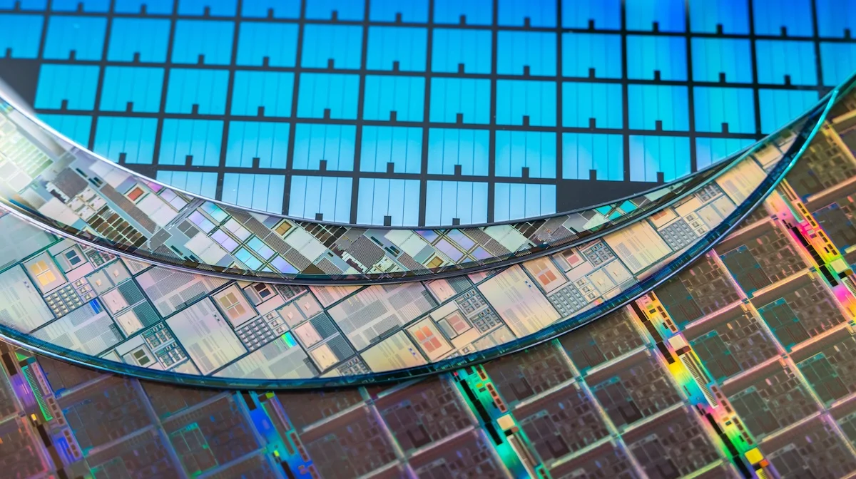
For decades, the semiconductor industry followed the trajectory of Moore’s Law, focusing primarily on the monolithic integration of transistors onto a single die. However, as the physical limits of silicon lithography are approached and the costs of single-die scaling skyrocket, the industry has turned toward heterogeneous integration. This approach allows designers to select the optimal process node for each specific function—such as using cutting-edge 2nm logic for processors while utilizing more cost-effective nodes for analog or power management components—and then "integrating" them into a single, high-performance package.
The Intel-led perspective highlights that since 2010, HI has transitioned from a niche solution for high-end servers to the backbone of the mobile and AI revolutions. Despite this, the authors identify a critical misalignment. Existing frameworks, such as the IEEE Heterogeneous Integration Roadmap, provide a foundational overview but often lack the granular, time-bound technical targets required for industrial synchronization. Without a unified 20-year vision, the global supply chain faces risks ranging from misallocated research funding to a lack of readiness in specialized materials and testing equipment.
Addressing the AI Energy and Scaling Bottleneck
The primary driver for this urgent call to action is the exponential growth of artificial intelligence. According to data cited by the research team, AI computing demands are currently doubling every three months. This trajectory is unsustainable under current hardware paradigms due to the "memory wall"—a phenomenon where the energy required to move data between the processor and memory exceeds the energy required for the actual computation.
In modern AI accelerators, the constant shuttling of data consumes upwards of 80% of total system power. Heterogeneous integration offers a direct solution through vertical stacking and dense interconnects. By placing High-Bandwidth Memory (HBM) directly on top of or adjacent to the logic die, the physical distance data must travel is reduced from centimeters to micrometers. This shift reduces latency and dramatically improves energy efficiency, but it also introduces extreme thermal density. The paper argues that unless thermal management and power delivery are co-designed at the roadmap level, the industry will hit a "thermal wall" that prevents further AI scaling regardless of transistor density.
A Chronology of Integration: From 2010 to 2026
The journey toward the current state of heterogeneous integration has been marked by several key milestones that have redefined the electronics ecosystem:
- 2010–2015: The Rise of 2.5D Packaging. Early adopters began using silicon interposers to connect logic and memory, primarily in high-end networking and graphics processing units (GPUs).
- 2016–2020: The Chiplet Revolution. Major semiconductor firms began disaggregating large monolithic designs into smaller "chiplets." This era saw the commercialization of advanced 3D stacking, allowing for higher yields and more flexible design cycles.
- 2021–2025: Hybrid Bonding and HBM Dominance. The industry moved toward hybrid bonding, which eliminates traditional solder bumps in favor of direct copper-to-copper connections, increasing interconnect density by orders of magnitude. This period also saw HBM become the standard for AI training hardware.
- 2026 and Beyond: The System-in-Package Era. The current phase, as defined by the Intel-led perspective, focuses on full system integration including photonics, integrated power regulation, and embedded cooling, requiring a multi-decade strategic plan.
Technical Gaps in Interconnects and Power Delivery
The research team identifies three specific pillars where current roadmaps are insufficient: interconnect density, power delivery, and thermal management.
In the realm of interconnects, hybrid bonding is the current gold standard. However, as pitches shrink below 10 micrometers, reliability becomes a significant concern. The authors emphasize the need for new modeling techniques to predict how these minute interfaces will behave over years of thermal cycling.
Simultaneously, power delivery has become a bottleneck. As chips draw hundreds of amps at sub-one-volt levels, the "power delivery network" (PDN) within the package must be revolutionized. The team suggests that integrating Gallium Nitride (GaN) power stages directly into the package could provide the necessary efficiency. Furthermore, as vertical integration intensifies, traditional air cooling is becoming obsolete. The perspective advocates for the integration of liquid cooling channels directly into the silicon stack—a move that requires unprecedented cooperation between material scientists and system architects.
Cross-Sector Collaboration and Global Stakeholders
One of the most notable aspects of the Nature Reviews Electrical Engineering publication is the breadth of its contributors. The collaboration includes industrial giants such as Texas Instruments, ASE (US) Inc., and Boeing; research powerhouses like the Lawrence Berkeley National Laboratory; and a wide array of academic institutions including UCLA, Purdue, and the University of Toronto.
This diverse coalition reflects the reality that HI is no longer just a "chip" problem; it is a "system" problem. For example, Boeing’s involvement highlights the critical need for HI in aerospace and defense, where components must survive "harsh environments"—extreme temperatures and radiation—that commercial-grade packaging is not traditionally designed to handle. The paper suggests that future roadmaps must create specific "qualification tiers" that allow commercial HI innovations to be rapidly adapted for specialized industrial and military use.
The Proposal for 20-Year Rolling Roadmaps
To bridge the identified gaps, the authors propose a new framework: the 20-year rolling roadmap. Unlike traditional five-year outlooks, a 20-year projection allows the industry to signal to materials suppliers and toolmakers what will be needed two decades in advance.
A central component of this proposal is the use of "Digital Twins." By creating high-fidelity virtual models of complex heterogeneous systems, engineers can simulate performance, thermal behavior, and mechanical stress long before a single wafer is processed. This approach is expected to reduce the time-to-market for new AI hardware and ensure that reliability is "baked in" to the design rather than addressed as an afterthought.
Broader Implications for the Global Electronics Ecosystem
The shift toward smarter, integrated systems rather than just larger chips has profound implications for the global economy. As AI continues to permeate every sector—from healthcare diagnostics to autonomous logistics—the efficiency of the underlying hardware will dictate the pace of societal adoption.
Furthermore, the integration of silicon photonics is poised to redefine data center architecture. By using light instead of electricity to move data between chips, photonics could solve the bandwidth limitations that currently plague large-scale AI clusters. The researchers argue that without a clear roadmap for photonics integration, the transition from electrical to optical signaling will be fragmented and inefficient.
In conclusion, the Intel-led perspective serves as a call to arms for the semiconductor industry. The transition to heterogeneous integration represents the most significant change in electronics manufacturing since the invention of the integrated circuit. By moving toward a coordinated, quantified, and long-term roadmapping strategy, the global electronics ecosystem can ensure that the "intelligence" in artificial intelligence is matched by the "intelligence" of the hardware that supports it. The authors make it clear: the future of computing will not be found on a larger piece of silicon, but in the sophisticated, three-dimensional union of diverse technologies working as one.
