

The global semiconductor industry is currently navigating a pivotal transition in interconnect technology as traditional scaling reaches its physical and mechanical limits. Copper-to-copper (Cu-Cu) hybrid bonding has emerged as the critical solution to meet the unprecedented interconnect density requirements of modern computing, yet the transition introduces rigorous sensitivities to surface topography and chemical contamination. As generative artificial intelligence (AI), autonomous systems, and industrial IoT continue to generate massive datasets, the demand for higher bandwidth and lower latency has forced engineers to move beyond conventional solder-based packaging toward direct metallic fusion.
The move toward copper-to-copper bonding is fundamentally driven by an insatiable global appetite for data. Large language models (LLMs) and generative AI tools are currently trained on datasets that encompass a significant portion of the public internet, requiring massive throughput between memory and processing units. Similarly, autonomous vehicles rely on a constant stream of high-resolution data from internal and external sensor arrays, while industrial "Smart Factories" monitor thousands of variables in real-time. This explosion in data volume creates a "memory wall," where the speed at which data moves between components becomes the primary bottleneck for system performance. From the architecture of individual microchips to the layout of global data centers, bandwidth is now the defining constraint for 21st-century circuit and systems design.
A Chronology of Interconnect Evolution
To understand the necessity of hybrid bonding, one must look at the historical trajectory of semiconductor packaging. For decades, wire bonding was the industry standard, utilizing thin gold or aluminum wires to connect chips to their frames. As the need for higher I/O counts grew, the industry shifted toward flip-chip technology and solder bumps (C4 bumps). These micro-bumps allowed for connections across the entire surface of the die rather than just the periphery.
However, as transistors continued to shrink and the industry moved toward 3D integrated circuits (3D-ICs) and chiplet architectures, the limitations of solder became apparent. At interconnect pitches below 20 micrometers (µm), solder bumps face reliability issues; the volume of material is insufficient to ensure a robust mechanical and electrical connection. Furthermore, the formation of copper-tin intermetallic compounds at these scales can lead to increased electrical resistance or sudden mechanical failure.
The first major response to this was thermocompression bonding (TCB), which utilizes copper studs on opposing surfaces fused by heat and pressure. While TCB provided an incremental improvement, it introduced its own set of challenges. The high temperatures and pressures required for TCB can cause interconnects to buckle or shift, leading to performance degradation. Additionally, the presence of copper studs increases the overall vertical thickness of the package, which is counterproductive for slim mobile devices and high-density server racks.
The Technical Shift to Hybrid Bonding
Hybrid bonding, often referred to as direct copper-to-copper bonding, represents the most advanced stage of this evolution. Unlike TCB, hybrid bonding places two chips or wafers flush against each other, creating a dielectric-to-dielectric and metal-to-metal bond simultaneously without any intervening solder or adhesive. This method maximizes interconnect density and minimizes vertical thickness, allowing for the stacking of multiple layers of logic and memory with near-seamless integration.
The scalability of hybrid bonding is its most significant advantage. While early implementations targeted a 10 µm pitch, the industry is rapidly pushing toward sub-micron levels. Recent demonstrations by researchers at imec, the world-leading research and innovation hub in nanoelectronics and digital technologies, have successfully showcased hybrid bonding with interconnect pitches as low as 400 nanometers (nm). This represents a generational leap in density that is essential for the future of High-Bandwidth Memory (HBM) and advanced logic stacking.
Surface Engineering and Contamination Control
Despite its conceptual simplicity—pressing two clean surfaces together to form a bond—hybrid bonding is notoriously difficult to execute at scale. The process requires an "active" yet "clean" surface, a state that is difficult to maintain in a standard manufacturing environment. Under ambient conditions, metallic copper reacts with oxygen to form a native oxide layer, which acts as an insulator and prevents effective bonding.
Current industry standards for hybrid bonding involve the use of plasma or thermal activation on silicon dioxide (SiO2) surfaces to create a hydrophilic, hydroxyl-terminated (-OH) layer. When two such surfaces are brought into contact, they form O-Si-O bonds at the interface at relatively low temperatures. To address the copper oxidation issue, a citric acid rinse is typically employed to strip the native oxide before the bonding process begins.

However, the quality of the bond ultimately depends on the rate of copper surface diffusion. Research from Osaka University has highlighted the importance of copper’s crystalline structure in this process. While it was initially theorized that nanotwinned copper would facilitate more rapid diffusion, simulations have shown that twin boundaries can actually stabilize the surface and prevent necessary atomic rearrangement. In contrast, nanocrystalline structures with a high density of grain boundaries have shown superior performance in void closure and grain growth across the bonding interface.
Managing Topography and the Role of CMP
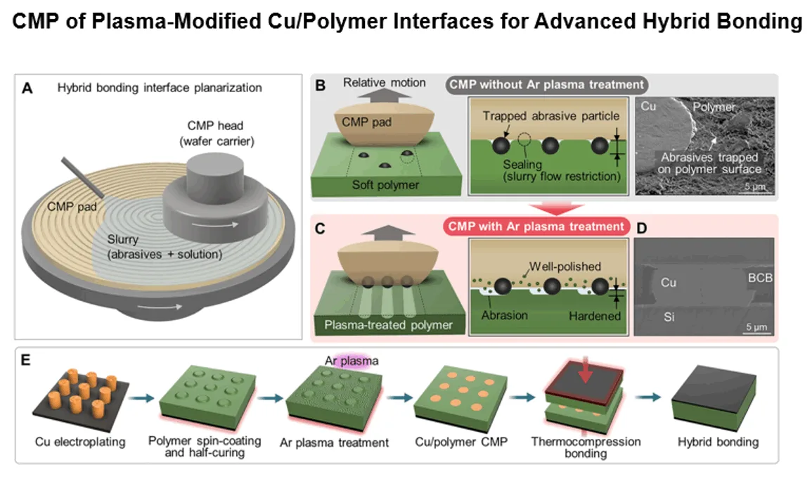
Beyond chemical cleanliness, surface topography is the most critical factor in determining the success of a hybrid bond. Because copper has a higher coefficient of thermal expansion (CTE) than silicon dioxide, it expands more significantly when heated. To account for this, engineers utilize Chemical Mechanical Polishing (CMP) to create a specific profile where the copper pads are slightly recessed—often by only a few nanometers—within the planar SiO2 surface.
If the "dishing" (recession) of the copper is too shallow, the expanding metal can create excessive stress, leading to delamination or cracking. If the dishing is too deep, the copper surfaces may never make contact, resulting in an open circuit. Achieving this level of precision requires advanced CMP slurries and pads, as well as real-time metrology to ensure uniformity across the entire wafer.
The mismatch in CTE between copper and traditional dielectrics like SiO2 remains a persistent challenge, particularly for large features such as Through-Silicon Vias (TSVs). This has led to the exploration of alternative dielectrics. Silicon Carbon Nitride (SiCN) has emerged as a promising candidate, with studies from imec indicating that SiCN offers higher bonding strength and better thermal stability compared to SiO2.
Innovations in Materials and Vacuum Processing
As the industry looks toward the next five years, new materials and processes are being integrated to further lower bonding temperatures and improve yield. Some research groups are experimenting with self-assembled monolayers (SAMs) to protect copper surfaces during the preparation of the surrounding dielectric. The challenge here lies in removing the monolayer completely before bonding without re-oxidizing the copper.
Another approach involves the use of passivating metal layers, such as silver or ruthenium. These metals are less prone to oxidation and are compatible with copper. Because they are conductive, they can remain at the interface without hindering electrical performance, allowing the copper to diffuse through them to form a permanent bond.
Furthermore, the introduction of compliant polymers like benzocyclobutene (BCB) is being explored to reduce bonding stress. Research led by Sukkyung Kang has demonstrated that while BCB is difficult to polish using traditional CMP, argon plasma treatment can harden the surface enough to allow for effective planarization. This creates a "wrinkled" surface that facilitates slurry flow and results in the desired topography for high-yield bonding.
Industry Implications and Strategic Outlook
The successful mass adoption of hybrid bonding has profound implications for the semiconductor supply chain. Currently, the process is predominantly handled by high-end foundries and integrated device manufacturers (IDMs) due to the extreme cleanliness requirements. However, as the technology matures, Outsourced Semiconductor Assembly and Test (OSAT) providers are increasingly investing in "cleanroom-plus" environments to compete in the advanced packaging space.
Industry analysts suggest that the cost of hybrid bonding—driven by the need for high-vacuum environments and high-precision alignment tools—will remain a barrier for mid-range applications in the short term. However, for the high-performance computing (HPC) sector, the performance gains are non-negotiable. NVIDIA’s latest Blackwell architecture and AMD’s 3D V-Cache technology are prime examples of products where advanced interconnects are essential for maintaining market leadership.
In conclusion, copper-to-copper hybrid bonding is no longer a laboratory curiosity; it is a fundamental requirement for the next era of silicon integration. While challenges in surface science, topography management, and material selection persist, the industry’s trajectory is clear. By overcoming these mechanical and chemical hurdles, engineers are paving the way for 3D structures that will define the capabilities of artificial intelligence and high-speed computing for decades to come. The transition marks a shift from viewing packaging as a protective shell to treating it as a primary driver of semiconductor performance.
