
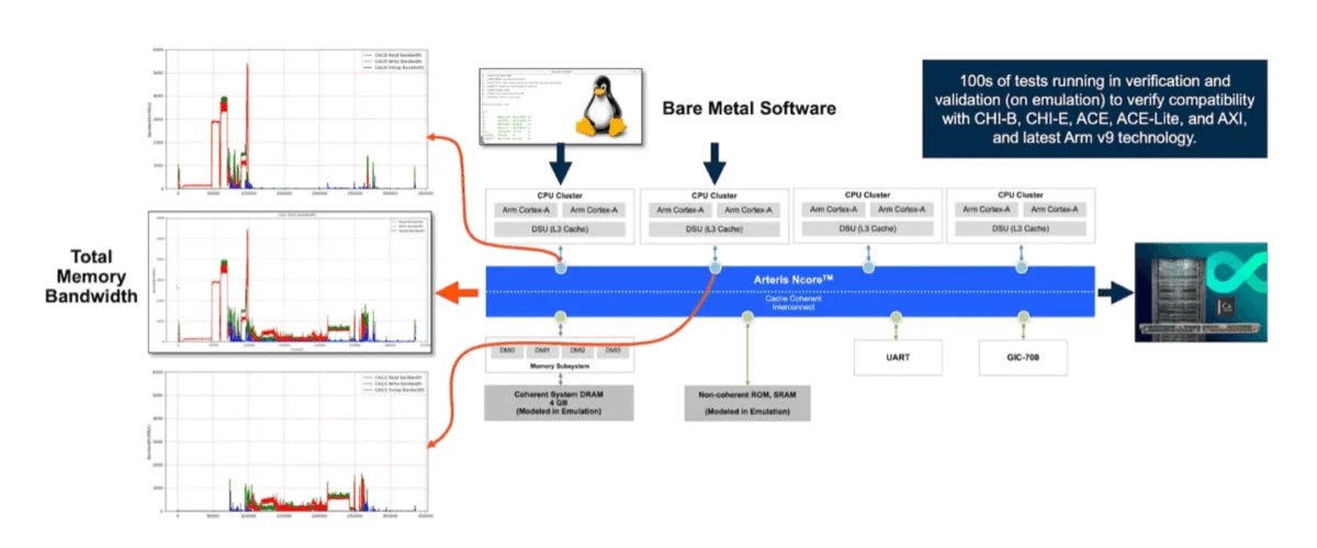

The rapid advancement of artificial intelligence and the widespread adoption of heterogeneous multi-die architectures have fundamentally shifted the priorities of semiconductor design, moving the focus from raw processing power to the efficiency of data movement. While leading-edge AI accelerators and high-performance computing (HPC) systems boast unprecedented teraflops of compute capability, these gains are increasingly susceptible to being neutralized by bottlenecks within the on-chip and between-die communication fabrics. As the industry moves away from monolithic system-on-chip (SoC) designs toward modular chiplet-based assemblies, the Network-on-Chip (NoC) has evolved from a simple structural layout into a sophisticated, hierarchical orchestration layer essential for maintaining system-level performance, thermal stability, and functional reliability.
The Shift Toward Heterogeneous Integration and Multi-Die Architectures
For decades, the primary challenge in chip design was wire congestion. As Moore’s Law enabled the placement of billions of transistors on a single die, the physical space required to route signals between blocks became a limiting factor. The traditional solution was the introduction of the Network-on-Chip, which replaced long, dedicated point-to-point wires with a shared, packet-switched communication infrastructure. However, the rise of generative AI and large language models (LLMs) has outpaced the scaling capabilities of monolithic silicon.
Modern AI workloads require massive memory bandwidth and low-latency communication between diverse processing elements, such as GPUs, CPUs, and specialized AI tiles. This has led to the "chiplet revolution," where functions previously housed on one die are split across multiple smaller dies connected via advanced packaging technologies like TSMC’s CoWoS (Chip-on-Wafer-on-Substrate) or Intel’s EMIB (Embedded Multi-die Interconnect Bridge).
According to Mick Posner, senior product marketing group director for chiplets and IP solutions at Cadence, the NoC was originally designed to address layout congestion on a single die. The new challenge is facilitating connections across die boundaries while ignoring the physical separation. Traditionally, NoCs were confined within the chip, relying on standard external protocols like PCIe to communicate with the outside world. In the current era of die-to-die (D2D) integration, the NoC must extend transparently across the package, effectively treating multiple physical dies as a single logical entity. This transition requires sophisticated protocols, such as AMBA CHI C2C (chiplet-to-chiplet), which allow for cache-coherent interfaces between different chips, such as an Arm-based CPU sitting adjacent to an Nvidia GPU.

A Chronology of Interconnect Evolution
The journey toward modern NoC architectures can be viewed through several distinct phases of technological development:
- Bus-Based Architectures (1990s – Early 2000s): Simple shared buses like the original AMBA protocols. These were effective for low-complexity chips but suffered from severe contention as the number of masters increased.
- Early NoC Integration (Mid-2000s – 2015): The introduction of packet-switched networks on silicon. Companies like Arteris and Sonics pioneered the use of routers and switches on-chip to manage data flow, primarily to solve physical routing congestion.
- The Coherency Era (2015 – 2020): As multi-core processing became standard, NoCs had to manage cache coherency across many cores. Protocols like AMBA 5 CHI (Coherent Hub Interface) emerged to maintain data consistency across distributed caches.
- The Chiplet and AI Era (2021 – Present): The current phase involves extending NoCs across die boundaries using high-bandwidth interfaces like UCIe (Universal Chiplet Interconnect Express). The NoC now manages not just data, but also power maps, thermal constraints, and multi-physics interactions across a 2.5D or 3D package.
The Complexity of Verification and Coherency
One of the most significant hurdles in modern NoC design is the management of mixed traffic types. Engineering teams must navigate the intricate balance between coherent and non-coherent data streams. Functional failures in these systems are rarely straightforward; instead, they often manifest as subtle performance degradations or, more catastrophically, as deadlocks during system bring-up.
Ashish Darbari, CEO of Axiomise, notes that a coherent request reordered behind a non-coherent stream might not appear as a failure during initial simulation. However, such an error can lead to a deadlock months later in the hardware, where the cost of rectification is astronomical. The boundary of the NoC has moved from the center of the die to the edge of the package, where timing, error handling, and retry semantics are fundamentally different.
Verification of these systems has become a "left-shift" priority. Frank Schirrmeister, executive director of strategic programs for system solutions at Synopsys, emphasizes that cache coherency is significantly more difficult to implement and verify than standard I/O coherency. The industry is moving toward automated test generation based on constraints, similar to the Portable Stimulus Standard (PSS), to determine if the NoC correctly identifies the location of the latest cache element across multiple cores and dies.
Multi-Physics Challenges and Thermal Management
The physical reality of multi-die systems introduces a new layer of complexity: multi-physics. NoCs are no longer just logical data paths; they are heat sources that interact with their neighbors. In a stacked 3D or 2.5D environment, the thermal activity in one chip can raise the baseline temperature of an adjacent chip.

Satish Radhakrishnan, head of GTM for semiconductor and electronics at Vinci, explains that global hotspots in a multi-die system may not coincide with any single chip’s local maximum. Traditional, sequential simulations run by specialists are becoming impractical because they cannot capture the full heat transfer path across the entire system. The industry requires a fundamentally different throughput model that can run physics simulations continuously across the full chip-to-system stack.
Furthermore, the mechanical stress of transient thermal loading can lead to physical defects. Issues such as warpage, low-K dielectric cracking, and delamination are genuine concerns for NoC architects. If a router node or a link fails due to mechanical stress, the NoC must be resilient enough to reroute traffic without system failure—a requirement that is particularly critical in safety-sensitive markets.
AI-Driven Traffic Patterns and Incast Bottlenecks
The nature of AI traffic is distinct from general-purpose computing. AI workloads often involve "incast" network bottlenecks, which occur during many-to-one communication phases. In data centers, after GPU clusters perform operations, they exchange data in patterns like "all-to-all" or "reduce ring."
Razvan Arhip, product manager for AI and network test solutions at Keysight Technologies, points out that these patterns create a high probability of congestion at specific entry points within the fabric. Testing these scenarios requires emulating the precise moments when traffic is fired across the network. Because real-world systems are never perfectly synchronized, testing environments must introduce randomization and jitter to see how protocols like RoCEv2 (RDMA over Converged Ethernet) or ECN (Explicit Congestion Notification) behave under stress.
Mission-Critical Reliability: Data Centers vs. Automotive
The requirements for NoC reliability vary significantly depending on the end market. In the data center, the focus is on maximizing throughput and minimizing GPU idle time. While wear-out is expected over time, the scale of the data center allows for some level of redundancy at the rack or cluster level.

In contrast, the automotive sector operates under much stricter constraints. As vehicles transition toward software-defined architectures and autonomous driving, the NoC becomes a safety-critical component. Kent Orthner, principal solutions architect at Baya Systems, highlights that in a self-driving car, a failure to recognize a pedestrian due to a network delay is unacceptable. Automotive-certified NoCs must include extra bits on every data path for error detection, redundant logic for parallel execution, and the ability to recover from failures within nanoseconds.
Broader Impact and Industry Implications
The evolution of NoC technology has profound implications for the semiconductor ecosystem. As the "interconnect wall" becomes a primary limiting factor for AI performance, we are seeing a shift toward Systems-Technology Co-Optimization (STCO). This approach requires architects to consider packaging, thermal management, and software-level traffic patterns simultaneously during the early stages of design.
Supporting data from industry analysts suggests that the market for chiplet-based designs is expected to grow at a compound annual growth rate (CAGR) of over 20% through 2030. This growth is driving a surge in demand for sophisticated NoC IP and EDA tools that can handle the massive capacity requirements. Matt Commens, senior director of product management at Synopsys, notes that companies are now demanding simulations of every single line in an interconnect—a task that requires unprecedented compute power but is necessary to ensure the integrity of high-speed signals.
Conclusion
The Network-on-Chip has transitioned from a background infrastructure component to a frontline architectural priority. As AI models continue to grow in complexity and the industry leans further into chiplet-based heterogeneous integration, the NoC will remain the defining factor in whether a system achieves its theoretical performance peaks or falls victim to data congestion. The integration of multi-physics simulation, formal verification, and application-specific reliability measures represents the new frontier of semiconductor engineering, ensuring that the movement of data remains as fast and reliable as the processors it serves.
