
The global power electronics industry is currently undergoing a foundational shift as researchers and manufacturers move beyond the limitations of silicon to embrace wide-bandgap semiconductors. While gallium nitride (GaN) has already established a firm foothold in the low-voltage consumer electronics market—most notably in the compact, high-efficiency chargers used for smartphones and laptops—its transition into high-voltage sectors like industrial power generation, electric vehicle (EV) drivetrains, and renewable energy grids has been more gradual. The primary challenge lies in the transition from lateral to vertical device architectures, a shift necessitated by the demanding requirements of kilovolt-level applications where reliability and power density are paramount.
The Physical Imperative for GaN Adoption
To understand the industry’s push toward GaN, one must look at the fundamental physics of semiconductor materials, specifically Baliga’s figure of merit. This metric serves as the primary benchmark for evaluating power devices, factoring in the dielectric constant, electron mobility, and the critical electric field. In wide-bandgap materials like GaN and silicon carbide (SiC), the critical electric field is approximately ten times higher than that of traditional silicon. This physical property allows GaN devices to handle significantly higher voltages within a much thinner drift layer, effectively reducing the resistance of the device.
While SiC has been the early leader in the high-voltage wide-bandgap market, GaN offers a different set of trade-offs that make it an attractive alternative for specific high-performance applications. For instance, SiC boasts superior thermal conductivity (4.9 W/cm-K compared to GaN’s 1.3 W/cm-K), which aids in heat dissipation. However, GaN possesses significantly higher carrier mobility (2,000 cm²/V-sec versus 900 cm²/V-sec for SiC). This higher mobility translates to faster switching speeds and lower switching losses, providing engineers with greater flexibility in designing high-frequency power systems that are both smaller and more efficient.
The Chronological Progression of GaN Technology
The journey of GaN from a laboratory curiosity to a commercial reality has spanned several decades, marked by distinct phases of development. In the late 1990s and early 2000s, GaN research was primarily focused on optical applications, leading to the revolution in blue LEDs and solid-state lighting. Because optical devices are physically small, they were less affected by the high dislocation densities found in early GaN material.
By the 2010s, the focus shifted toward power electronics. The industry initially favored lateral conduction designs, utilizing a two-dimensional electron gas (2DEG) formed at the interface of GaN and AlGaN. These lateral devices were relatively easy to manufacture on silicon substrates (GaN-on-Si) and were perfect for 65V to 650V applications. However, as the industry looked toward the 1,200V and 1,700V requirements of the heavy industrial and automotive sectors, the limitations of lateral designs became apparent. In a lateral device, the breakdown voltage is tied to the horizontal distance between the gate and the drain; increasing the voltage requires increasing the device’s footprint, which eventually becomes economically unviable.
Entering the 2020s, the focus has shifted toward vertical architectures. Much like traditional silicon and SiC MOSFETs, vertical GaN devices allow current to flow through the bulk of the material, meaning that breakdown voltage can be increased by simply making the epitaxial layers thicker without expanding the surface area of the chip. This transition represents the current frontier of GaN research and development.
Overcoming Substrate and Manufacturing Hurdles
The potential of vertical GaN has historically been constrained by the difficulty of manufacturing high-quality GaN substrates. Unlike silicon, which can be grown in massive, high-purity ingots, GaN is notoriously difficult to produce as a freestanding wafer. Most GaN devices are grown heteroepitaxially on silicon substrates. However, the lattice mismatch and differences in thermal expansion between GaN and silicon create immense internal stress.

Karen Geens, a lead researcher at imec, has noted that GaN-on-silicon substrates are often fragile and prone to breakage due to this mechanical stress. To mitigate this, researchers have turned to engineered substrates. One promising solution is Qromis Substrate Technology (QST). These wafers utilize a polycrystalline aluminum nitride (AlN) core encapsulated in specialized layers and topped with a single-crystalline silicon growth template. The QST approach more closely matches the thermal expansion coefficient of GaN, allowing for the growth of the thick GaN layers necessary for high-voltage vertical conduction without the catastrophic cracking seen in traditional GaN-on-Si methods.
Furthermore, the availability of GaN-on-GaN substrates—where GaN is grown on a native GaN seed—has improved significantly. While still more expensive than silicon or SiC, these native substrates offer the lowest possible dislocation densities, which is a prerequisite for reliable high-voltage operation in the kilovolt range.
The Doping Dilemma: Ion Implantation and Activation
One of the most significant technical barriers to complex vertical GaN structures is the process of selective doping. In silicon manufacturing, creating p-type and n-type regions via ion implantation is a mature technology. In GaN, however, the process is fraught with complications.
N-type doping in high-voltage GaN requires extremely low dopant concentrations, often one to two orders of magnitude lower than what is used in optical GaN devices. This precision is difficult to achieve because unintentional carbon contamination from metal-organic precursors acts as a background dopant, degrading carrier mobility and increasing resistance.

P-type doping, which typically uses magnesium (Mg), presents even greater challenges. Tetsu Kachi of Nagoya University has highlighted that carbon can act as both a donor and an acceptor in GaN, complicating the electrical profile of the device. Furthermore, the activation of magnesium dopants requires high-temperature annealing. Ryo Tanaka of Fuji Electric has reported that GaN surfaces begin to decompose at temperatures above 800°C. To achieve p-type activation, temperatures as high as 1,300°C are often required. This necessitates the use of protective AlN capping layers and innovative nitrogen implantation techniques to prevent the loss of nitrogen from the GaN lattice and to pin magnesium ions in their proper positions.
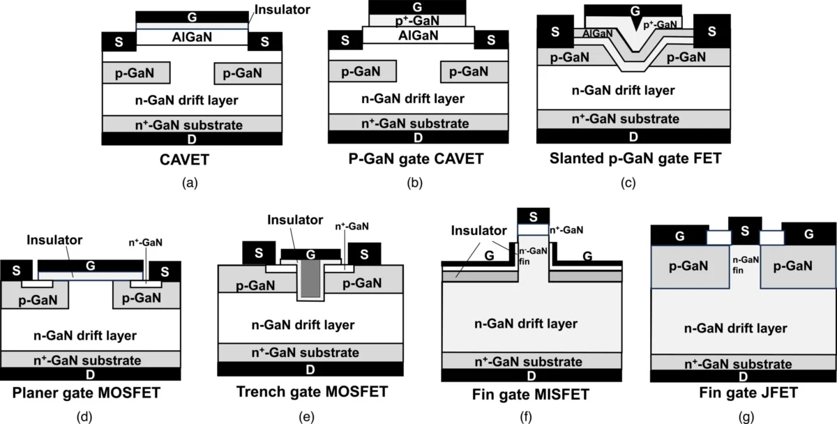
Advances in Vertical MOSFET Design and Dielectrics
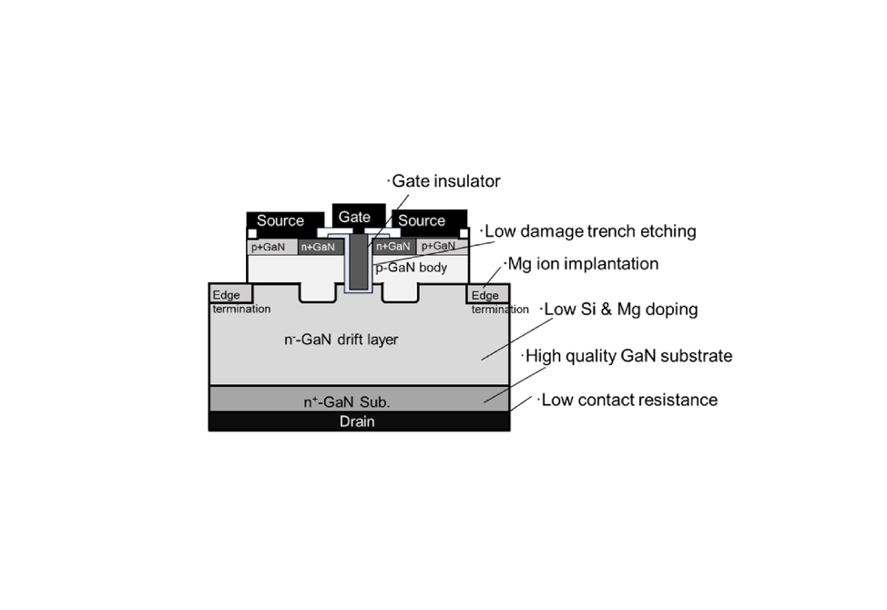
As the industry moves toward vertical designs, the trench gate MOSFET has emerged as a leading candidate for commercialization. This architecture is favored for its relatively straightforward fabrication process and high power density. However, the performance of these devices is heavily dependent on the quality of the trench etch and the gate dielectric.
Achieving flat, undamaged sidewalls in the trench is critical to ensuring a clean current path and high mobility. Researchers have found that a combination of Cl2 and SiCl4 etch gases provides the best results. The Cl2 reacts with the GaN to facilitate the etch, while the SiCl4 helps passivate the sidewalls, preventing electrical leakage.
The choice of gate dielectric is another area of intense competition. While aluminum oxide (Al2O3) is a common choice, many research groups, including those at the University of Padova, have found that an Al2O3/SiO2 bilayer offers better protection against breakdown. Thicker dielectrics help to mitigate the effects of surface traps, though they can also lead to higher threshold voltages. Recent experiments with AlSiO dielectrics deposited via plasma-enhanced atomic layer deposition (ALD) have shown promise, though achieving the theoretical limits of mobility remains an ongoing challenge for the industry.

Industry Implications and the Road Ahead
The successful commercialization of vertical GaN power devices would have profound implications for the global transition to a low-carbon economy. In the electric vehicle sector, vertical GaN could enable onboard chargers and inverters that are significantly lighter and more efficient than current SiC-based models, directly translating to increased driving range and faster charging times. In the realm of renewable energy, GaN-based inverters could reduce the energy losses associated with converting DC power from solar panels into AC power for the grid.
Despite the progress, expert consensus suggests that the "GaN revolution" for high-voltage applications is still in its refining phase. While the individual process modules—such as high-quality growth, ion implantation, and trench etching—are now largely in place, integrating them into a high-yield, cost-effective manufacturing flow remains the final hurdle.
The data suggests that while SiC currently holds the majority share of the high-voltage wide-bandgap market, GaN is positioned as a powerful successor or a high-performance alternative for specialized applications. As manufacturing costs for GaN-on-GaN and engineered substrates continue to fall, and as the industry converges on standardized vertical designs, GaN is expected to move from the fringes of high-voltage power management to the very center of the electrification movement. The future of power electronics is increasingly vertical, and gallium nitride is the material poised to define that trajectory.
