
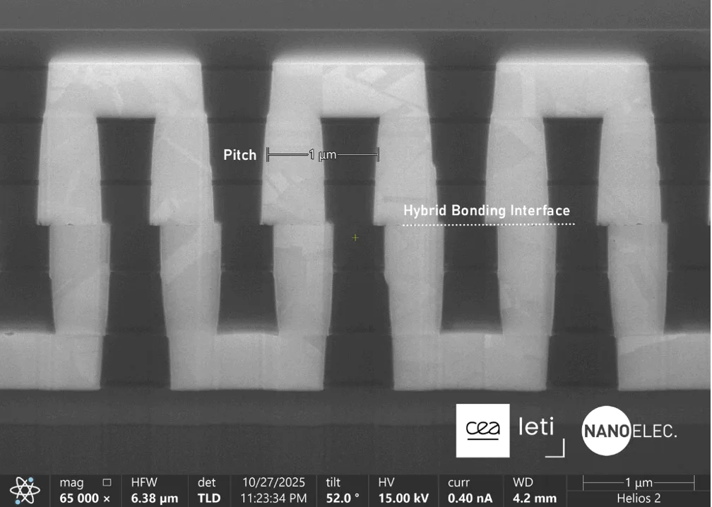

Hybrid bonding has successfully transitioned from a laboratory curiosity to a cornerstone of modern semiconductor production, yet the industry’s mastery of the technology is less comprehensive than current high-volume successes might suggest. While wafer-to-wafer (W2W) applications, such as CMOS image sensors, have demonstrated that meticulously prepared copper and dielectric surfaces can be reliably fused at scale, the sector now faces a more formidable challenge. The next frontier involves the integration of finer pitches, complex die-to-wafer (D2W) processing, and the assembly of heterogeneous products that combine logic, memory, and specialized functions. These components often feature disparate materials, dimensions, and thermal tolerances that were never originally intended to be identical, creating a multifaceted engineering hurdle for the global supply chain.
The Shift from Wafer-Level Parallelism to Die-Level Precision
The fundamental appeal of hybrid bonding lies in its ability to create extraordinarily dense interconnect populations by forming pads across a wafer in parallel. However, as the industry moves toward die-to-wafer bonding, it inherits the stringent requirements of wafer-level processing while introducing the mechanical complexities of handling individual chips. Unlike W2W bonding, where two entire patterned wafers are aligned and joined, D2W bonding requires each die to be screened, handled, aligned, and placed as a separate mechanical object.
This transition sacrifices the inherent parallelism of wafer-level processing for the flexibility of "Known Good Die" (KGD) selection. In a W2W flow, a single defect on one wafer can render the corresponding region on the second wafer useless, compounding yield losses. D2W bonding avoids this by ensuring only functional dies are integrated into the final stack. However, this advantage comes at a steep price: the throughput of individual placement is significantly lower, and the risk of contamination or misalignment increases every time a die is handled.
The physical bond itself forms at the conclusion of a multi-step progression, but its success is a reflection of every process that preceded it. Variables such as copper recess depth, dielectric topography, film stress, wafer warpage, and the cleanliness of the environment all contribute to an "error budget." While each individual process may operate within its specified tolerance, their cumulative variation can narrow the process window to a point where repeatable, high-volume manufacturing (HVM) becomes impossible.
Chronology of Hybrid Bonding Evolution and Pitch Scaling
The journey of hybrid bonding began in the early 2000s, pioneered by companies like Ziptronix (now part of Adeia), focusing primarily on low-density applications. By the mid-2010s, the technology found its first major commercial success in CMOS image sensors, where W2W bonding allowed for the stacking of sensing layers directly onto logic layers.
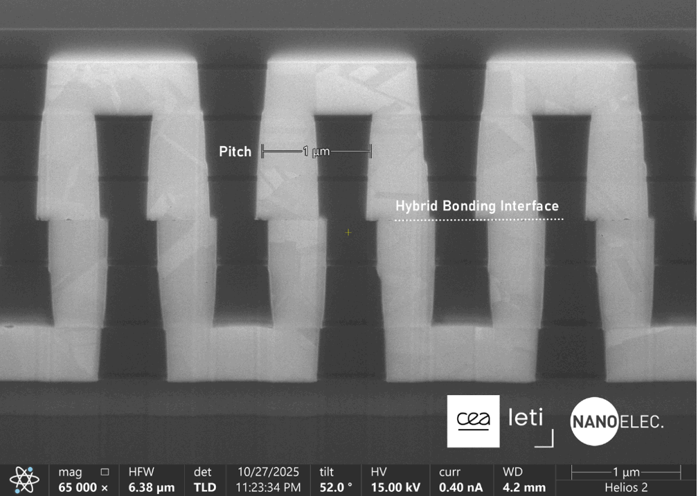
As of 2024, the industry has reached a pivotal juncture. Currently, the commercially viable "sweet spot" for hybrid bonding pitch is approximately 6 $mu$m. While laboratory environments have successfully demonstrated pitches as fine as 1 $mu$m or even sub-micron levels, the transition to HVM at these dimensions remains a long-term target. The disparity between roadmap targets and production reality is driven by the economic necessity of yield. A 6 $mu$m logic-to-memory interface provides substantial system-level performance gains today, justifying the cost of manufacturing controls, whereas the move to 1 $mu$m requires a generational leap in cleanroom standards and placement accuracy.
The Technical Complexity of the "Glass-to-Glass" Interface
One of the most significant challenges in hybrid bonding is the lack of physical compliance at the interface. Traditional microbump technology utilizes solder, which can melt and deform to accommodate slight variations in height or small particles. Hybrid bonding, conversely, is essentially a glass-to-glass and copper-to-copper interface.
"It only takes one nanosized particle, and you basically lift the glass off, and you’ve messed up a whole bunch of units on the wafer," notes Mike Kelly, Vice President of Chiplets and FCBGA Integration at Amkor. Because the dielectric surfaces must achieve intimate contact to initiate the bond, any local obstruction creates a "void" that can span an area much larger than the particle itself.
This sensitivity necessitates a radical rethinking of the assembly environment. For years, Outsourced Semiconductor Assembly and Test (OSAT) providers have operated in environments that are significantly less stringent than front-end wafer fabs. Bringing hybrid bonding to the back-end requires the implementation of localized "mini-environments" or ISO Class 1 clusters within existing facilities. Converting an entire OSAT into a front-end-style cleanroom would be economically prohibitive, yet the alternative—localized extreme cleanliness—requires sophisticated engineering to manage the transition of materials between different zones.
Geometry, Warpage, and the Role of Temporary Carriers
The mechanical state of a die at the moment of bonding is rarely the same as its state during initial wafer processing. As wafers are thinned and attached to temporary carriers for backside processing, they are subjected to thermal cycles and mechanical stresses. The choice of carrier material—be it glass or silicon—and the properties of the temporary adhesive are critical. If the Coefficient of Thermal Expansion (CTE) between the carrier and the device wafer is not closely matched, the resulting warpage can consume the entire alignment margin.
Furthermore, the singulation process—cutting the wafer into individual dies—releases internal stresses, often causing the die to "potato chip" or warp. When these dies are presented to the bonder, they may possess non-linear distortions that a standard placement tool cannot easily correct. Research presented by Intel Foundry indicates that factors such as chiplet thickness and bonder nozzle geometry play a significant role in managing these distortions. Advanced modeling and finite-element analysis are increasingly used to predict how a die will behave under the force and vacuum of the bonding tool, allowing engineers to compensate for geometric errors before they lead to yield loss.
Thermal Budgets and the Challenge of Heterogeneous Integration
The final stage of the hybrid bonding process is the anneal, which serves two purposes: it strengthens the dielectric-to-dielectric bond and causes the recessed copper pads to expand and fuse. Traditionally, this requires temperatures between 300°C and 400°C for several hours.
While these temperatures are standard for logic wafers, they pose a significant threat to other components. High Bandwidth Memory (HBM) and certain photonic or RF devices can suffer performance degradation or physical damage when exposed to prolonged heat at 400°C. Consequently, there is an industry-wide push toward low-temperature hybrid bonding.
Recent developments from research institutes like CEA-Leti have demonstrated successful bonding at temperatures as low as 100°C. Achieving high electrical yield at these lower temperatures requires a delicate balance of surface activation chemistry and precise copper topography. The goal is to find the lowest possible thermal budget that still ensures long-term reliability and low contact resistance.
Industry Implications: The Need for Organizational Transparency
The move toward fine-pitch hybrid bonding is forcing a shift in how the semiconductor ecosystem collaborates. In traditional packaging, the boundaries between the material supplier, the equipment manufacturer, and the fab are clearly defined by "black box" specifications. However, the margins in hybrid bonding are now so thin that these boundaries are becoming blurred.
A cleaning chemistry developed by one company must be perfectly tuned to the Chemical Mechanical Polishing (CMP) pads of another and the placement sequence of a third. If a material supplier changes a formulation, it can have unforeseen effects on the "bond-wave" behavior inside the equipment. Industry leaders, including representatives from Mitsubishi Chemical and Lam Research, argue that faster iteration and successful HVM will require a new level of transparency across the supply chain.
This need for a "shared language" extends to the design phase. Currently, there is no universal Advanced Packaging Design Kit (ADK) that governs how pad layouts and keep-out regions should be handled across different foundries and OSATs. Standardizing these design rules is essential for the broad adoption of chiplet-based architectures, as it allows designers to mix and match dies from different sources with the confidence that they will bond successfully.
Conclusion: A Connected Process for a Connected Future
The successful scaling of fine-pitch hybrid bonding will not be achieved by perfecting a single machine or a single chemical formula. Instead, it requires the industry to view the bond as the final expression of a singular, connected process that begins at the initial design and continues through to final test.
As the industry moves toward 1 $mu$m pitches and beyond, the distinction between "front-end" and "back-end" manufacturing will continue to erode. The companies that succeed in this environment will be those that can master the accumulation of small deviations—managing particles, warpage, and thermal budgets with unprecedented precision. Hybrid bonding has already proven its worth in the world of image sensors; its next act will be to redefine the limits of high-performance computing, memory, and the very architecture of the modern microchip.
