

The semiconductor industry is currently navigating a pivotal transition in memory architecture as traditional embedded Flash (eFlash) reaches its physical scaling limits at the 28nm process node. As chipmakers push toward FinFET and GAA (Gate-All-Around) architectures at 16nm, 7nm, and beyond, the inability to effectively scale eFlash has created a vacuum now being filled by a new generation of non-volatile memory (NVM) technologies. Among the leading contenders, Magnetic RAM (MRAM) and Resistive RAM (RRAM) have emerged as the primary successors, while specialized technologies like Ferroelectric RAM (FeRAM) and the nascent UltraRAM aim to disrupt the broader memory landscape, including the potential replacement of DRAM.
The Scaling Wall and the Decline of Embedded Flash
For decades, NOR Flash was the industry standard for non-volatile storage in microcontrollers (MCUs) and System-on-Chips (SoCs). However, the physics of Flash memory—which requires high-voltage charge pumps and thick oxide layers—becomes prohibitively difficult to integrate into advanced CMOS logic processes below 28nm. Integrating eFlash into FinFET nodes requires a significant increase in mask layers, leading to higher manufacturing costs and reduced yields.
Industry leaders, including major foundries like TSMC, Samsung, and GlobalFoundries, have recognized that the effort to shrink Flash is no longer economically or technically viable. This realization comes at a time when the global supply of standalone Flash is increasingly constrained. According to Sean Dougherty, vice president of sales at Everspin, the demand for high-bandwidth memory (HBM), DRAM, and NAND is so intense that major suppliers are prioritizing high-volume AI and data center clients, effectively decommitting from smaller or more specialized industrial markets. This supply crunch has accelerated the adoption of alternative NVM technologies that can be integrated into the Back-End-of-Line (BEOL) of semiconductor manufacturing.
The Rise of MRAM and RRAM in the FinFET Era
MRAM and RRAM are not merely replacements for Flash; they represent a fundamental shift in how data is stored and accessed. Both technologies are BEOL-compatible, meaning they can be built between the metal layers of a chip with minimal additional processing steps. This compatibility allows designers to integrate memory into advanced logic platforms with only a few extra mask layers—typically two to four—compared to the ten or more required for eFlash.
Magnetic RAM (MRAM): The Performance Leader
MRAM operates by utilizing the magnetic orientation of electrons to store data. Spin-Transfer Torque (STT) MRAM is the current commercial standard, offering fast read and write speeds, high endurance, and excellent data retention in harsh environments.
Suhail Zain, vice president of regional marketing at UMC, notes that MRAM is frequently positioned for high-endurance, high-speed use cases, such as persistent working memory. Its ability to withstand extreme temperatures and radiation has made it the preferred choice for aerospace, defense, and automotive applications. Jamie Schaeffer, vice president of product management at GlobalFoundries, highlights that MRAM read access times are approaching 10 picoseconds, making it a potential candidate for last-level cache (LLC) applications, which could alleviate the "memory wall" created by the poor scaling of Static RAM (SRAM).

Resistive RAM (RRAM): The Cost-Effective Alternative
While MRAM leads in performance, RRAM is winning the race for general-purpose, cost-sensitive applications. RRAM functions by creating or dissolving conductive filaments within a dielectric material. The industry has largely coalesced around Oxide-based RRAM (OxRAM) due to its compatibility with standard CMOS materials and its lower risk of contamination in high-volume fabs.
Infineon and TSMC have recently made significant strides in commercializing RRAM for automotive microcontrollers. Robert Wiesner, a distinguished engineer at Infineon, reports that their RRAM implementation can maintain data for over 1,000 hours at 175°C, a critical requirement for automotive safety standards. RRAM’s smaller footprint and simpler manufacturing process make it an ideal replacement for code storage in IoT devices, power management ICs (PMICs), and entry-level microcontrollers.
The Displacement of Phase-Change RAM
While MRAM and RRAM thrive, Phase-Change RAM (PCRAM) appears to be falling out of favor for embedded applications. Once considered a frontrunner—and famously used in Intel’s Optane memory—PCRAM has struggled to scale to FinFET nodes.
Synopsys, a leader in memory compilers, indicates that customer demand for embedded PCRAM has vanished. "There’s not been enough demand from any customer that says, ‘I want to be able to embed it,’" says Daryl Seitzer, principal product manager at Synopsys. Without a roadmap to smaller nodes, PCRAM is likely to remain confined to older planar CMOS technologies or specialized niche markets.
FeRAM and the Quest for Infinite Endurance
Ferroelectric RAM (FeRAM) has long been the "dark horse" of the memory world. It offers the highest endurance of any NVM and consumes significantly less power during write operations because it relies on electric fields rather than current flow. Historically, FeRAM was limited by its use of Lead Zirconate Titanate (PZT), a material that is difficult to scale and incompatible with modern CMOS fabs.
However, a breakthrough involving Hafnium Zirconium Oxide (HZO) has revitalized the technology. CEA-Leti has successfully demonstrated FeRAM at the 22nm node using HZO, which is already a common material in advanced high-k metal gate stacks. This makes FeRAM a potential candidate for ultra-low-power edge AI devices and continuous data logging where energy efficiency is paramount. If current research at the 5nm and 4nm nodes proves successful, FeRAM could bridge the gap between NVM and DRAM.
UltraRAM: A Quantum Leap in Memory Design
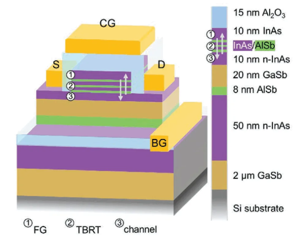
Perhaps the most radical development in the sector is UltraRAM, a technology being pioneered by the startup Quinas. Unlike other NVMs that rely on resistance or magnetism, UltraRAM uses compound semiconductors (III-V materials) and quantum resonant tunneling.

UltraRAM utilizes a floating gate structure similar to Flash, but instead of forcing electrons through a dielectric oxide—a process that eventually damages the material—it uses quantum mechanics to allow electrons to tunnel through a triple-barrier structure at low voltages. Peter Hodgson, CTO of Quinas, explains that this "gentle" programming method results in an effectively infinite lifetime. Testing has shown no degradation after 10 million cycles, and data retention is projected to exceed 1,000 years.
With predicted switching speeds of 1 nanosecond at the 20nm node, UltraRAM is the first non-volatile technology that could realistically challenge DRAM. While it currently requires III-V foundries, which are more common in the laser and photodiode industries, Quinas is working on integration strategies that would allow these bit cells to be bonded to silicon control logic.
Comparative Data and Industry Trajectory
The transition to these new memories is supported by robust performance data. The following table summarizes the current state of embedded NVM technologies:
| Technology | Primary Use Case | Scaling Potential | Key Advantage |
|---|---|---|---|
| MRAM | Automotive, Industrial, Cache | Down to 5nm | High speed, high reliability |
| RRAM | IoT, Consumer MCUs, PMICs | Down to 12nm | Low cost, small footprint |
| FeRAM | Data Logging, Ultra-low power | Researching < 10nm | Extremely high endurance |
| UltraRAM | High-performance Computing | 20nm (Predicted) | DRAM speed with non-volatility |
| eFlash | Legacy Microcontrollers | Stuck at 28nm | Proven, mature ecosystem |
Broader Implications for the Semiconductor Ecosystem
The diversification of the memory landscape has profound implications for chip design and system architecture. As SRAM fails to scale, the density of modern SoCs is increasingly dominated by memory, leading to larger die sizes and higher costs. The integration of MRAM as a high-density, non-volatile alternative to SRAM could drastically reduce the physical footprint of AI accelerators and edge processors.
Furthermore, the rise of "In-Memory Computing" (IMC) is being fueled by these new bit cells. Both RRAM and UltraRAM have shown the potential to support multi-level states, allowing them to perform neural network weight storage and multiplication within the memory array itself. This architecture eliminates the energy-intensive process of moving data between the processor and memory, which is the primary bottleneck in modern AI workloads.
The industry’s shift toward these technologies is no longer a matter of "if" but "when." Foundries like TSMC and Samsung have already integrated MRAM and RRAM into their long-term roadmaps for the 12nm and 6nm nodes. As these technologies mature and production volumes increase, the cost per bit will continue to drop, further eroding the remaining advantages of legacy Flash.
By 2029, when Quinas expects to bring UltraRAM to market and FeRAM research hits the 5nm mark, the distinction between "working memory" (DRAM) and "storage memory" (Flash) may begin to blur. The result will be a new generation of "universal memory" devices that are faster, more reliable, and significantly more energy-efficient than the systems of today.
