
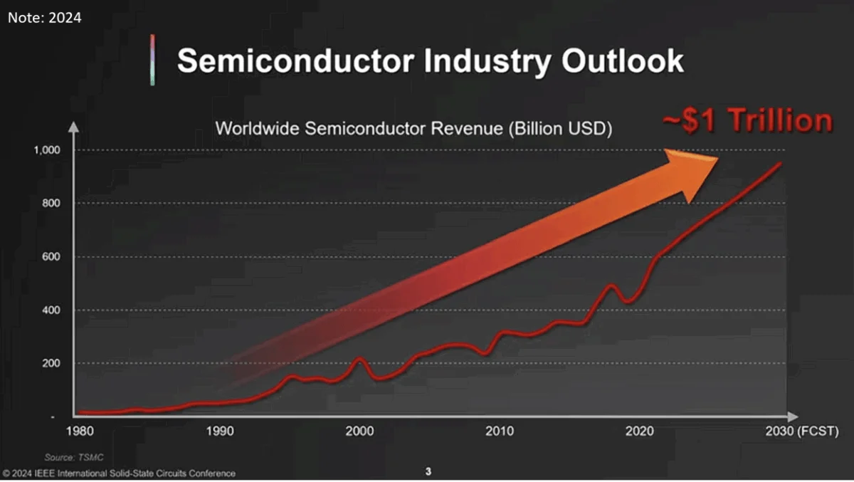

The global semiconductor landscape is undergoing a transformation of historic proportions, with the industry rapidly approaching a projected $1.7 trillion valuation by the end of 2026. This monumental shift, highlighted during last week’s TSMC Open Innovation Platform (OIP) North America Technology Symposium, underscores a departure from traditional growth models. Driven by the voracious compute and energy demands of artificial intelligence, the sector is currently experiencing a surge that has eclipsed even the most optimistic forecasts made just two years ago.

A Rapidly Evolving Forecast
In January 2024, at the International Solid-State Circuits Conference (ISSCC), TSMC’s leadership projected that the worldwide semiconductor market would reach approximately $1 trillion by 2030. At the time, this was viewed as an ambitious, if not bold, roadmap. However, the trajectory of the industry has been fundamentally altered by the generative AI boom.
During the OIP symposium, TSMC North America CEO Sajiv Dalal announced that the industry is now on track to hit $1.7 trillion by the close of 2026. Of this total, AI-specific hardware is expected to command more than $1 trillion, effectively cementing artificial intelligence as the primary engine of global silicon demand. This outlook aligns closely with recent data from Gartner, which also anticipates a $1.6 trillion market valuation by 2026, signaling a consensus among industry analysts regarding the ferocious pace of AI-driven capital expenditure.

Chronology of Accelerated Innovation
The path to this valuation is paved with significant technological milestones. TSMC’s recent financial performance serves as a barometer for the broader industry; the company reported a 53.3% year-over-year revenue increase as of August 2026. When comparing the first eight months of 2025 to the same period in 2026, the company recorded a 39.3% increase, reflecting a massive scaling of production capacity.
This growth is not merely a result of higher volumes but is deeply tied to the rapid adoption of advanced nodes. Li-Pen Yuan, vice president of business development at TSMC, noted that the industry has seen a four-fold increase in new tape-outs (NTOs) when measuring the second year of technology cycles across the N5, N3, and N2 processes. The N2 node, in particular, is witnessing an unprecedented number of new design starts, outpacing the design velocity previously seen with the N3 node. This indicates that hardware designers are increasingly comfortable and reliant upon bleeding-edge lithography to meet the complex requirements of modern AI models.

Addressing the Scaling Bottlenecks
As AI models scale, they create intense pressure on three primary vectors: compute performance, memory density, and power efficiency. L.C. Lu, TSMC senior fellow and vice president for design and technology platforms, highlighted that inference token usage has surged 500-fold over the last three years. This shift in demand—from training large models to the high-volume deployment of inference—has turned inference efficiency into the most critical factor for hardware development.
To address these constraints, TSMC is leveraging new architectural approaches. The introduction of the A14 Nanoflex technology, for instance, offers a 1.5x cell height reduction, providing a 14% speed improvement and a 23% reduction in power compared to the N2P node. Such granular improvements in power efficiency are vital, as the thermal and energy limits of current data center architectures threaten to stall the AI build-out.

Furthermore, the industry is looking to radically optimize memory throughput. TSMC has presented a figure of merit based on the product of transistor count, speed, and power efficiency. By 2029, the industry is expected to achieve an 87-fold improvement in this benchmark. Projections suggest that within five years, HBM (High Bandwidth Memory) bandwidth will increase 34-fold, while 3D DRAM and SRAM bandwidths are expected to see massive gains of 115-fold and 830-fold, respectively. These advancements are essential for minimizing the "memory wall" that currently limits the throughput of large-scale AI accelerators.
The Rise of SiP and Advanced Packaging
The symposium also signaled a structural shift in chip architecture. Greg Dix, vice president of engineering for Broadcom’s ASIC Products Division, noted during a panel discussion that the era of the traditional System-on-Chip (SoC) is yielding to the System-in-Package (SiP) era. The increased complexity of AI accelerators, which often combine diverse compute, memory, and networking dies, requires sophisticated packaging technologies that integrate multiple components into a single, high-performance unit.

The development of OpenAI’s "Jalapeno" custom AI ASIC serves as a case study for this new era. The project moved from initial kick-off to final tape-out in just nine months, a velocity that was previously considered impossible for a custom silicon project of that magnitude. This rapid turnaround is enabled by the "positive feedback loop" currently present in the industry, where AI-driven EDA (Electronic Design Automation) tools are being used to design the next generation of AI chips.
Communication Infrastructure: The COUPE Milestone
As data processing speeds increase, the bottleneck is increasingly shifting to data movement. To mitigate this, TSMC is pushing forward with its COUPE (Compact Universal Photonic Engine) technology. This platform is designed to enable energy-efficient, high-speed optical communication, essential as serial data rates move toward 224G and 448G. By integrating silicon photonics, TSMC-COUPE aims to address the growing energy-per-bit requirements of hyperscale data centers. The roadmap for COUPE includes significant increases in gigabits per second (Gbps) capacity, utilizing multiple wavelengths per fiber to exponentially increase bandwidth without a proportional increase in energy consumption.

Ecosystem Collaboration and the Future of Design
The complexity of these designs has necessitated a deeper integration within the semiconductor ecosystem. TSMC’s OIP Cloud Alliance, which now includes managed-cloud services from Amazon Web Services (AWS) and Microsoft Azure, facilitates mixed-partner EDA workflows that are essential for modern chip development. The recent addition of imec as a partner, and the recognition of IC-Link for its role in cloud-managed design services, highlights how the industry is decentralizing the design process while relying on standardized, high-performance platforms.
To further accelerate time-to-market, TSMC is rolling out AI Design Kits (ADK). These kits are designed to automate and optimize design flows, allowing human engineers to focus on architectural innovation while AI agents handle the complex, iterative tasks of physical design and verification. This framework represents the next evolution of semiconductor design, where artificial intelligence is not only the product but also the architect of the silicon it runs upon.

Strategic Implications
The findings from the OIP symposium suggest that the semiconductor industry is no longer merely a supporting player in the global economy but the foundational infrastructure for the AI-driven future. The transition from $1 trillion to $1.7 trillion in revenue in just a few years represents a structural expansion, not a cyclical one.
For stakeholders, the implications are profound. The shift toward SiP architectures, the critical reliance on advanced packaging, and the integration of silicon photonics suggest that companies which can successfully navigate these technological pivots will command significant market share. Meanwhile, the rapid cycle of design and tape-out—as evidenced by the Broadcom and OpenAI collaboration—implies that the competitive advantage will go to those who can best leverage AI-driven design methodologies. As the industry moves toward 2030, the ability to manage power efficiency and memory density at the sub-nanometer scale will remain the ultimate determinant of success in the global technology race.
