
The global semiconductor landscape is currently undergoing a period of rapid transformation, driven by the dual pressures of artificial intelligence (AI) integration and the escalating complexity of hardware-level security. As the industry moves toward the 2026 conference season, including the IEEE/JSAP Symposium on VLSI Technology and Circuits and the International Symposium on Computer Architecture (ISCA), several key developments have emerged across electronic design automation (EDA), advanced packaging, and workforce policy. These shifts reflect a broader move toward "More than Moore" scaling, where performance gains are achieved not just through transistor density, but through heterogeneous integration and AI-driven design optimization.
Standardizing AI for Electronic Design Automation
A significant milestone in the evolution of design tools occurred this week as Si2 released its AI for EDA Ontology. This framework is designed to provide a standardized example ontology and a set of use cases specifically tailored to enable experimentation with EDA agentic systems. In the context of chip design, an ontology serves as a structured vocabulary that allows different AI tools and human engineers to share a common understanding of data relationships. As EDA companies increasingly integrate generative AI and autonomous agents into their workflows to handle tasks like floorplanning and routing, the lack of standardized data structures has been a primary bottleneck. Si2’s release aims to harmonize how AI agents interpret design intent, potentially accelerating the time-to-market for complex system-on-chips (SoCs).
In tandem with software advancements, hardware providers are showcasing the capabilities of modern mobile silicon. Arm, in collaboration with Sumo Digital, announced a new mobile game titled "Neural Dawn." The project serves as a technical showcase for GPU neural graphics technology, demonstrating how machine learning-enhanced rendering can bring desktop-level visual fidelity to mobile devices without exceeding the strict thermal and power envelopes of handheld hardware.
Breakthroughs in Advanced Packaging and RF Systems
As traditional scaling slows, the industry is looking toward advanced packaging and new material science to maintain the trajectory of performance. Imec, the Belgium-based research hub, announced two major breakthroughs this week. First, it introduced a narrowband receiver chip compliant with the IEEE 802.15.4ab Ultra-Wideband (UWB) standard. This chip reportedly achieves a fourfold extension in UWB range, which has significant implications for precise indoor positioning and secure "find my device" applications. Secondly, Imec revealed progress in laser-bonding III-V chiplets onto 300mm RF silicon interposers. This technique allows for the integration of high-performance compound semiconductors—essential for 5G-Advanced and 6G communications—directly onto standard silicon CMOS wafers, bridging the gap between high-frequency performance and mass-market manufacturability.
In the commercial sector, Qnity Electronics expanded its portfolio for organic interposer applications. The company introduced multi-role copper and dry film photo-imageable dielectric materials designed to enhance the reliability of advanced packages. Furthermore, Qnity released its Optivision Max CMP (Chemical Mechanical Planarization) pads, which feature improved defect control and extended lifespans, addressing the high-volume manufacturing needs of foundries producing AI accelerators.
Addressing the critical "power wall" in data centers, Lotus Microsystems launched its V-Strata platform. This vertical power delivery and thermal management solution is designed to sit directly beneath AI processors. By moving power delivery closer to the silicon, the system reduces resistive losses and improves thermal dissipation, which is vital as AI server racks approach power densities of one megawatt. Simultaneously, Innosilicon debuted its UALink (Universal Accelerator Link) IP, featuring a single-lane 112G/224G PHY, providing a high-speed interconnect fabric necessary for scaling multi-chiplet AI training clusters.

Emerging Research in Lithography and Memory Compatibility
Academic and institutional research continues to push the boundaries of what is physically possible in semiconductor manufacturing. Researchers at the University of Osaka have utilized advanced simulations to optimize tin-plasma Extreme Ultraviolet (EUV) lithography sources. Their findings suggest that mid-infrared solid-state lasers could significantly improve conversion efficiency. This discovery is a critical step toward making future EUV systems smaller and more energy-efficient, potentially lowering the barrier to entry for sub-2nm node production.
In the realm of non-volatile memory, a team led by Georgia Tech demonstrated that oxide-channel Ferroelectric Field-Effect Transistors (FeFETs) can survive annealing temperatures up to 650°C (1,202°F). This thermal stability is a prerequisite for making emerging non-volatile memory (eNVM) compatible with the rigorous 3D NAND manufacturing process. If successfully integrated, this could lead to significantly faster and more durable storage solutions for edge AI devices.
Thermal management at the chip level also saw innovation from MIT. Researchers there successfully integrated Gallium Nitride (GaN) dielets into a single-crystal diamond interposer. Diamond, known for its superior thermal conductivity, acts as a heat spreader that normalizes the temperature across the die. This allows transistors to operate at peak performance levels for longer durations without compromising long-term reliability—a breakthrough for high-power RF and power electronics.
Additionally, DARPA’s THREADS program (Thermal Management Technologies for Heterogeneous Integration) demonstrated a fivefold increase in RF system power density. This advancement could effectively double the range of current radar systems, showcasing the strategic importance of thermal innovation in defense and aerospace applications.
The Escalating Threat Landscape in Hardware Security
Security remains a primary concern for the industry, with new vulnerabilities highlighting the risks inherent in hardware interconnects. Researchers at ETH Zurich reported a third exploitation of a vulnerability in AMD’s confidential computing architecture. The team suggested that hardware interconnects are becoming a preferred attack surface for sophisticated actors, necessitating a shift in how secure enclaves are designed and verified.
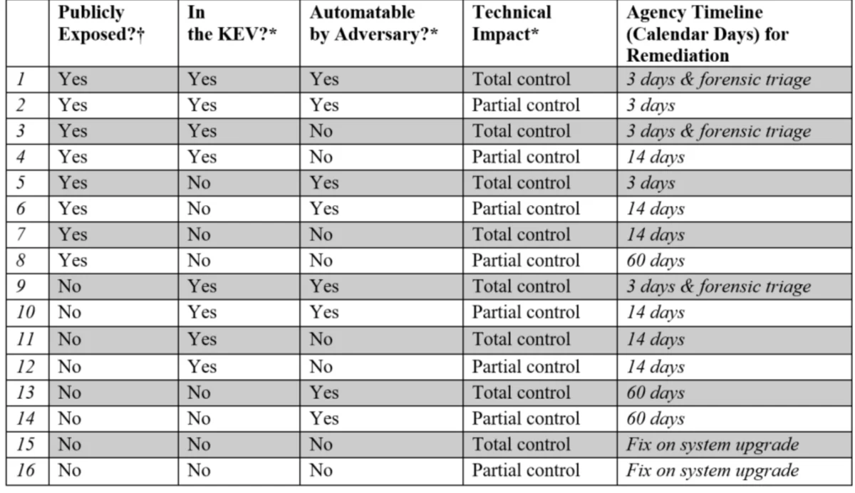
The Cybersecurity and Infrastructure Security Agency (CISA) has responded to the increasing speed of cyberattacks by shortening remediation deadlines for federal agencies. Agencies now have only three days to patch the most critical vulnerabilities. CISA cited concerns that AI-driven tools are allowing attackers to weaponize newly disclosed flaws faster than ever before. This policy shift underscores the urgency of maintaining robust "security-by-design" principles.
In terms of active threats, Lumen’s Black Lotus Labs identified a resurgence of the JDY botnet. This China-linked network consists of compromised small-office/home-office (SOHO) routers and IoT devices used to map exposed services for rapid exploitation. On the software side, Check Point warned of active exploits targeting CVE-2026-50751, a critical authentication-bypass flaw in certain VPN protocols, while Microsoft issued a massive wave of security updates covering everything from Windows Secure Boot to UEFI and kernel components.

To aid the defensive community, Todd Austin of the University of Michigan has made his Simon cipher library open-source. The release includes SystemVerilog implementations and a fuzzer, providing hardware designers with verified tools to implement lightweight cryptography in resource-constrained IoT devices.
Workforce Development and the Global Talent War
The semiconductor industry’s growth is currently constrained by a significant talent shortage, prompting new initiatives in education and policy. The University of Florida introduced the PATHS (Preparing the Autistic Population Toward Hardware Security) program. This initiative provides hands-on training and mentorship for neurodivergent students, aiming to integrate a traditionally underutilized talent pool into the integrated circuit (IC) industry.
Corporate giants are also stepping in to fill the gap. Meta announced America’s Workforce Academy, a $115 million free training program focused on AI data center jobs. Meanwhile, Siemens and ABB have formed the Careers Electric Coalition to scale the U.S. electrical workforce, recognizing that the transition to an electrified economy requires a massive influx of skilled technicians.
However, the industry faces headwinds from shifting immigration policies. The Hoover Institution warned that tighter H-1B and student-visa rules risk pushing STEM talent and AI startups to overseas competitors. A recent federal court ruling struck down a $100,000 fee on new H-1B petitions—originally proposed by the previous administration—calling it an unlawful tax. This legal victory for the tech sector highlights the ongoing tension between national security-focused immigration policies and the industry’s need for global talent.
The Path to Fault-Tolerant Quantum Computing
Quantum computing is moving closer to practical utility, with a focus on error correction. Alice & Bob, a leader in the field, introduced its first complete quantum system available for research. The system is notable for its ability to create a logical qubit using as few as 18 physical qubits—a significant improvement over other architectures that require thousands. The company also proposed a new framework to benchmark logical qubit claims, aiming to bring transparency to the competitive quantum hardware market.
In the public sector, Silicon Quantum Computing (SQC) received an additional $28 million in funding to continue its work on high-precision silicon quantum chips. Furthermore, IQM proposed a novel quantum error-correcting code that lowers logical error rates while requiring fewer physical qubits, further signaling that the industry is shifting its focus from "qubit count" to "qubit quality" and fault tolerance.
As the industry prepares for the upcoming VLSI and ISCA symposiums, the convergence of AI, advanced materials, and rigorous security protocols defines the new era of semiconductor engineering. The ability to integrate these disparate technologies into a cohesive, secure, and manufacturable system will determine the leaders of the next decade’s technology stack.
