
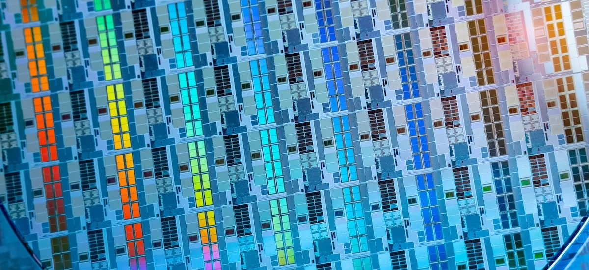
The semiconductor industry is currently undergoing a fundamental architectural shift as the traditional monolithic System-on-Chip (SoC) reaches the physical and economic limits of Moore’s Law. As transistors approach the 2nm and 1.8nm nodes, the cost of manufacturing large, single-die chips has skyrocketed, while the yield rates for these massive dies have plummeted. In response, the industry has pivoted toward multi-die systems, often referred to as chiplets or 3D Integrated Circuits (3D-ICs). This transition, however, introduces a monumental challenge: the management of logical and physical interconnectivity between multiple dies, interposers, and substrates. Achieving seamless communication between these components requires the precise planning and automation of hundreds of thousands, and increasingly millions, of microbumps and Through-Silicon Vias (TSVs).
The Engineering Challenge of Massive Interconnect Scales
In a multi-die environment, the physical interface between dies is the primary bottleneck for both performance and manufacturability. Traditionally, microbumps—small solder balls used to connect a die to a substrate or another die—have been the standard. However, as the demand for higher bandwidth and lower power consumption increases, the number of these connections has exploded. While a standard mobile processor a decade ago might have required a few thousand pins, modern high-performance computing (HPC) and AI accelerators are pushing toward designs that feature millions of interconnects.
The complexity of managing these connections manually is no longer feasible. Engineers must account for signal integrity, power delivery, thermal management, and mechanical stress, all while ensuring that the physical layout of the bumps aligns perfectly across multiple layers of the stack. A single misalignment in a TSV or a microbump can render an entire multi-thousand-dollar wafer useless. This has necessitated a new generation of Electronic Design Automation (EDA) tools capable of automating the planning, visualization, and analysis of these dense interconnect arrays.
Evolution of Interconnect Technology: From MCM to Hybrid Bonding
The journey to today’s complex 3D-IC structures has been defined by the steady reduction of interconnect pitch—the distance between the centers of two adjacent connections.
The Chronology of Packaging Evolution
- 1980s–1990s: Multi-Chip Modules (MCM): Early attempts at multi-die integration used standard organic substrates to connect separate chips. The interconnect density was low, and the primary goal was reducing the footprint on the Printed Circuit Board (PCB).
- 2000s: System-in-Package (SiP): This era saw the introduction of wire bonding and basic flip-chip technologies to stack dies, primarily for memory (NAND/DRAM) applications.
- 2010s: 2.5D Integration and Silicon Interposers: The introduction of High-Bandwidth Memory (HBM) necessitated the use of silicon interposers. This allowed for much finer routing than organic substrates, utilizing TSVs to pass signals through the interposer to the substrate.
- 2020–Present: 3D-IC and Hybrid Bonding: We are now entering the era of "true" 3D integration. Technologies like TSMC’s SoIC (System on Integrated Chips) and Intel’s Foveros utilize hybrid bonding, which eliminates the solder bump entirely in favor of direct copper-to-copper connections.
As the industry moves from microbumps (with pitches typically ranging from 40 to 25 microns) to hybrid bonding (with pitches shrinking below 10 microns and eventually to 1 micron), the number of connections per square millimeter increases by orders of magnitude. This density shift is the primary driver for the automation requirements outlined in recent industry white papers and technical specifications.
Supporting Data: The Shrinking Pitch and Increasing Density
The move toward higher interconnect density is supported by aggressive scaling targets from the world’s leading foundries. According to industry data, the transition from traditional flip-chip to microbumps allowed for a connection density of approximately 400 to 1,600 connections per square millimeter. With the advent of advanced microbump technology, this increased to nearly 10,000 per square millimeter.
However, hybrid bonding represents a quantum leap. By removing the need for solder caps, hybrid bonding allows for:
- Pitch Scaling: Reduction from 30μm to less than 5μm.
- Interconnect Density: Over 1,000,000 connections per square millimeter.
- Parasitic Reduction: A significant decrease in inductance and capacitance, which translates to lower power consumption per bit transferred.
Managing a million connections per square millimeter requires EDA tools that can handle massive databases without latency. Visualization tools must allow designers to "see" through multiple layers of silicon to identify potential routing conflicts or thermal hotspots that could compromise the integrity of the TSVs.
Automation and Productivity in EDA Workflows
The primary goal of automating bump and TSV planning is to improve engineering productivity. In traditional workflows, bump placement was often handled in a spreadsheet or a static 2D CAD tool, which was then manually reconciled with the physical design. In a multi-die system, this "siloed" approach is prone to catastrophic errors.

Modern automation platforms provide a unified 3D environment where the die, the interposer, and the package are designed concurrently. Key features of these automated systems include:
- Feasibility Analysis: Early-stage tools that determine if the required number of signals can physically fit within the designated area given the pitch constraints.
- Auto-Routing: Algorithms that automatically route signals from the die’s core logic to the appropriate bump or TSV, optimizing for shortest path and minimal interference.
- Cross-Die Checking: Real-time verification that ensures a bump on "Die A" perfectly aligns with the landing pad on "Die B" or the interposer.
- Thermal and Stress Simulation: Automated analysis of how the heat generated by the logic die affects the mechanical reliability of the TSVs, which are susceptible to cracking due to Coefficient of Thermal Expansion (CTE) mismatches.
Official Responses and Industry Strategic Alignment
Leading EDA providers, such as Synopsys, have emphasized that the "Shift Left" methodology—performing analysis and verification earlier in the design cycle—is critical for multi-die success. In recent technical forums, industry experts have noted that the complexity of 3D-IC design is shifting the responsibility of packaging from the end-of-line assembly houses to the front-end chip designers.
"The scale of interconnectivity in modern AI chips is staggering," noted a senior director of engineering at a leading silicon design firm during a recent industry symposium. "We are no longer just designing a chip; we are designing a vertical system. Without automated planning for bumps and TSVs, the time-to-market would stretch from months to years."
Foundries like TSMC and Samsung have also released updated design kits (PDKs) that specifically include parameters for automated 3D stacking. These kits are designed to work seamlessly with EDA tools to ensure that the "Golden Rule" of semiconductor manufacturing—design for manufacturability (DFM)—is maintained even at the million-interconnect scale.
Broader Impact and Implications for the Global Economy
The ability to automate and successfully execute multi-die designs has implications far beyond the engineering lab. It is a critical enabler for the next generation of artificial intelligence. Large Language Models (LLMs) and generative AI require massive amounts of memory bandwidth, which can only be provided by HBM stacks connected via dense TSV arrays to the processor.
Furthermore, the "chiplet" revolution allows for heterogeneous integration, where a designer can combine a 3nm logic die with a 7nm I/O die and a specialized analog die, all in one package. This approach reduces costs and allows for more specialized, efficient computing. However, the glue that holds this heterogeneous system together is the interconnect. If the planning of bumps and TSVs is not optimized, the efficiency gains of using chiplets are lost to the overhead of power-hungry, slow inter-die communication.
Future Outlook: The Path to Sub-Micron Interconnects
Looking forward, the roadmap for bump and TSV planning will continue to track toward the sub-micron level. Research into "bumpless" bonding and sequential 3D integration (where transistors are built on top of each other on the same wafer) is already underway. These future technologies will likely push the interconnect count into the tens of millions.
To keep pace, EDA tools will need to incorporate more advanced machine learning algorithms to predict routing congestion and thermal issues before they occur. The integration of "digital twins"—virtual models of the physical chip stack—will become standard practice, allowing for real-time monitoring of the design’s health throughout the lifecycle.
In conclusion, the automation of bump and TSV planning is not merely a convenience for designers; it is a fundamental requirement for the continued advancement of semiconductor technology. As the industry moves toward more complex, multi-layered architectures, the tools and methodologies used to manage millions of interconnects will define the leaders in the next era of silicon innovation. The white papers and technical frameworks being established today by leaders like Synopsys provide the essential blueprint for navigating this increasingly vertical landscape.
