
The Escalating Challenge of Memory Density and Advanced Nodes
At the heart of the modern computing revolution is the relentless drive for higher density. As the industry moves from 5nm to 3nm and eventually 2nm process nodes, the physical dimensions of memory cells—primarily Static Random-Access Memory (SRAM)—have scaled to the point where traditional manufacturing tolerances are no longer sufficient to guarantee stability. Increased density brings a host of parasitic effects, including higher leakage currents, increased susceptibility to electromagnetic interference, and thermal hotspots that can degrade performance over time.
In modern SoC designs, memory typically occupies more than 50% of the total die area, and in some AI-optimized processors, this figure can climb as high as 80%. Consequently, the yield of the entire chip is inextricably linked to the yield of its memory components. If a single block of memory is non-functional and cannot be repaired, the entire silicon die may have to be discarded, leading to significant economic losses. This reality has forced a move away from "one-size-fits-all" testing toward highly specialized, application-aware strategies.
The Shift Toward Hierarchical Testing Architectures
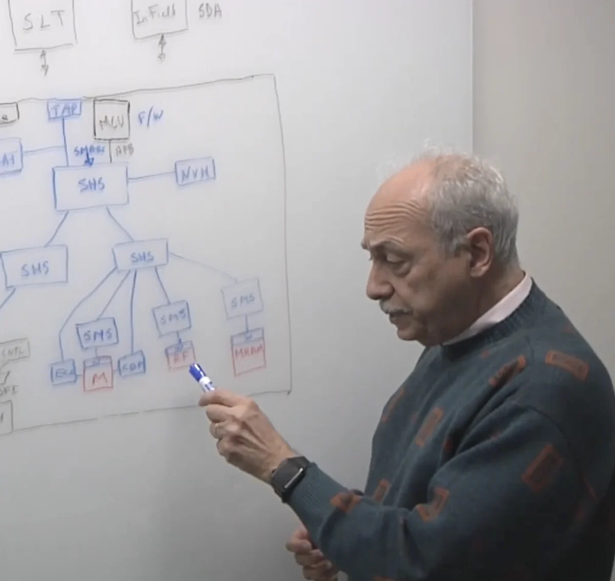
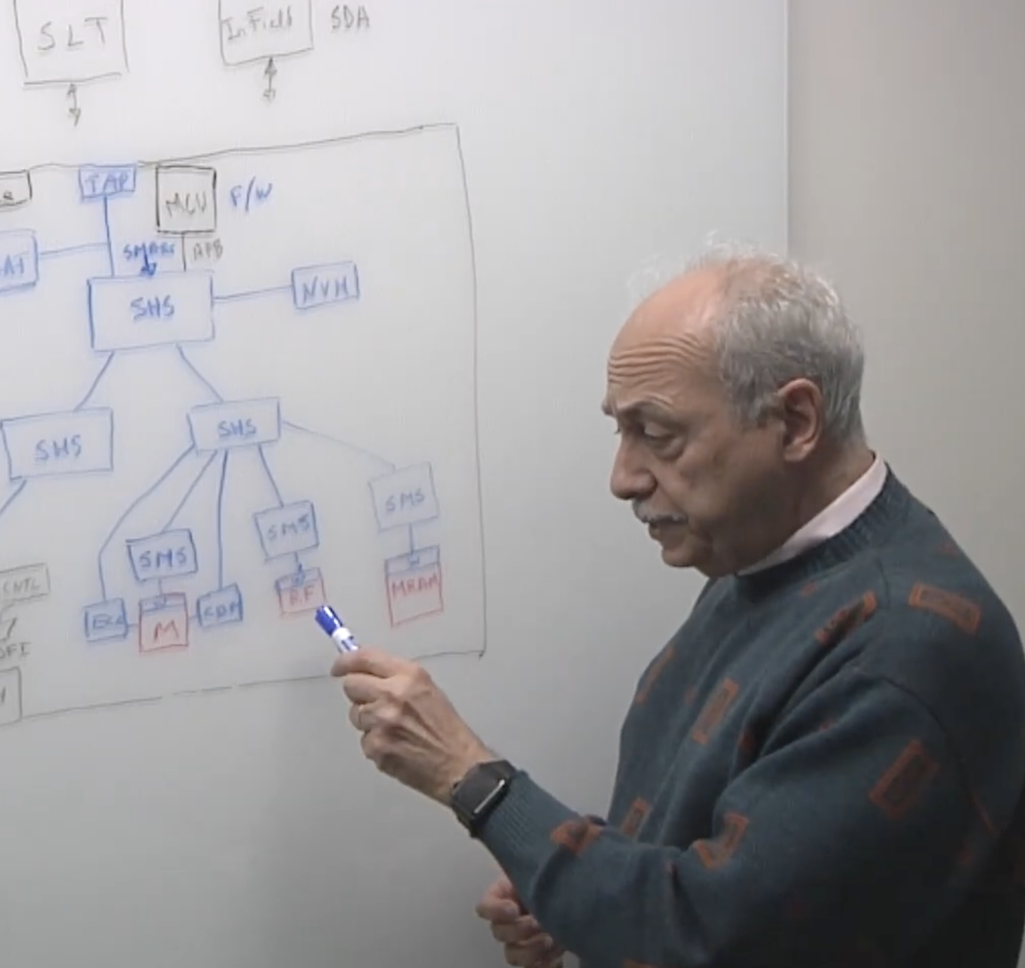
Yervant Zorian, chief architect and fellow at Synopsys, emphasizes that the industry is moving toward a hierarchical approach to memory testing. In previous generations, memory testing was often treated as a peripheral activity conducted at the end of the manufacturing process using Automatic Test Equipment (ATE). However, the sheer volume of memory in modern chips makes external testing prohibitively expensive and time-consuming.
A hierarchical approach involves embedding test and repair capabilities directly into the silicon at multiple levels. This begins at the individual memory wrapper level, extends to the memory cluster level, and finally integrates into the full system-level test architecture. By distributing the intelligence of the test infrastructure, designers can isolate specific memory banks, run parallel tests, and implement real-time repairs without taxing the primary processor or requiring external hardware.
This hierarchy is particularly critical in multi-die assemblies, such as those using High Bandwidth Memory (HBM) or chiplet-based architectures. In these configurations, memory is often stacked vertically or placed on a silicon interposer. Testing these structures requires "known good die" (KGD) strategies, where memory is verified before assembly, after bonding, and throughout its operational life in the field.
Chronology of Memory Testing Evolution
To understand the current state of the art, it is necessary to examine the chronological evolution of memory testing technologies:
- The 1990s: External ATE Dominance. Testing was primarily conducted by large, external machines that interfaced with the chip’s pins. Memory was relatively small, and simple "March" algorithms were sufficient to detect most physical defects.
- The early 2000s: The Rise of BIST. As memory moved deep inside the SoC, external pins could no longer access it directly. Built-In Self-Test (BIST) became standard, allowing the chip to test itself using internal logic.
- The 2010s: BISR and Redundancy. With the shrinking of process nodes, manufacturing defects became more common. Built-In Self-Repair (BISR) was introduced, using redundant rows and columns of memory cells to "patch" defective areas identified during BIST.
- The 2020s: Silicon Lifecycle Management (SLM). We have entered an era where testing does not end at the factory gate. Continuous monitoring, in-system testing, and predictive analytics are now used to manage the health of memory throughout the life of the product, from the data center to the autonomous vehicle.
The Impact of AI and Variable Workloads
The rollout of AI across every sector of technology has introduced new variables into the memory reliability equation. AI workloads are characterized by massive data throughput and high "toggling" rates, which place immense stress on memory subsystems. Unlike traditional general-purpose computing, AI applications often run at maximum thermal envelopes for extended periods.
This creates a phenomenon known as "silent data corruption," where bit-flips occur not due to a permanent manufacturing defect, but due to transient environmental factors or aging. For instance, high temperatures can cause a memory cell to lose its charge more quickly, leading to errors that might not be caught by standard power-on self-tests.
To combat this, the industry is adopting workload-aware testing. This involves simulating the specific patterns of an AI algorithm—such as the heavy read/write cycles of a Large Language Model (LLM)—during the design phase to identify which memory blocks are most likely to fail under stress. Testing is no longer just about finding broken wires; it is about ensuring signal integrity under maximum load.
Supporting Data: The Cost of Memory Failure
Industry data underscores the urgency of these advanced testing methodologies. According to recent market analysis:
- Yield Impact: Memory-related defects account for up to 40% of yield loss in advanced logic chips.
- Economic Scale: The global memory market is projected to exceed $200 billion by 2026, driven largely by AI demand. Even a 1% improvement in yield through better repair mechanisms can result in hundreds of millions of dollars in saved costs for a major foundry.
- Reliability Standards: In the automotive sector, the ISO 26262 standard requires a "Single Point Fault Metric" (SPFM) of over 99% for safety-critical systems. Achieving this without sophisticated in-system memory testing is virtually impossible.
Multi-Physics Simulations and Digital Twins
As Yervant Zorian notes, the complexity of modern memory systems requires more than just logical testing; it requires massive multi-physics simulations. A memory chip is not just an electrical circuit; it is a thermal and mechanical entity. In a 3D-stacked HBM cube, the heat generated by the bottom layers must pass through the top layers to be dissipated. If the thermal expansion of the different materials is not perfectly synchronized, the micro-bumps connecting the dies can crack.

Digital twins—virtual replicas of the physical chip—are now used to model these interactions. By running a digital twin in parallel with the design process, engineers can predict how a memory array will react to voltage fluctuations, thermal spikes, and physical stress. This allows for the creation of "guard bands"—safety margins that ensure the memory remains functional even as it ages or operates in harsh environments.
Official Responses and Industry Alignment
Major players in the semiconductor ecosystem have signaled a unified approach to these challenges. Synopsys, through its Silicon Lifecycle Management (SLM) platform, has integrated testing and repair tools that span from RTL design to field operation. Similarly, foundries like TSMC and Samsung have introduced specialized "Design for Test" (DFT) guidelines for their 3nm and 2nm processes, emphasizing the need for embedded sensors that monitor memory health in real-time.
At recent industry forums, representatives from hyperscale data center operators (such as Google and Meta) have called for more transparent memory health reporting. These end-users require "fleet-level" diagnostics to identify failing memory modules before they cause system crashes in the cloud, further driving the demand for standardized in-system test protocols.
Broader Implications for the Future of Technology
The implications of memory testing and repair extend far beyond the laboratory. In the realm of autonomous robots and smartphones, the ability to "self-heal" memory is a prerequisite for long-term reliability. As consumers hold onto their devices longer, and as industrial robots are expected to operate for decades, the silicon must be able to compensate for the inevitable degradation of transistors.
The move toward hierarchical, multi-physics-based testing represents a fundamental change in the philosophy of semiconductor manufacturing. We are moving from a "build and verify" model to a "monitor and adapt" model. In this new paradigm, memory is not a static component but a dynamic subsystem that is constantly being evaluated, optimized, and repaired by the very silicon it inhabits.
As AI continues to push the boundaries of what is possible in silicon, the innovations in memory testing led by experts like Zorian will be the invisible foundation upon which the next generation of computing is built. Without the ability to ensure every bit is stored correctly and every failure is repaired instantly, the promise of the AI era—from autonomous driving to personalized medicine—cannot be fully realized. The future of the industry lies in its ability to turn "test and repair" from a final hurdle into a continuous, intelligent process.
