
The semiconductor industry is currently undergoing a fundamental structural transformation as the limits of monolithic system-on-chip (SoC) designs become increasingly apparent in the face of artificial intelligence (AI) and high-performance computing (HPC) demands. For decades, the monolithic approach—where all functional blocks of a chip are integrated onto a single silicon die using a uniform process node—was the industry standard due to its straightforward design flow and high intra-chip communication speeds. However, as AI models grow in complexity, requiring unprecedented levels of compute density and memory bandwidth, the monolithic model has hit a "reticle limit." This physical boundary, dictated by the maximum size a lithography machine can print on a wafer (typically around 858mm²), has forced architects to seek alternative methods of scaling.
In response, the industry has pivoted toward chiplet-based architectures. Unlike their monolithic predecessors, chiplet designs disaggregate the SoC into smaller, functional components that can be manufactured independently. This modular approach allows designers to use the most appropriate process node for each specific function; for instance, high-performance logic can be built on cutting-edge 3nm nodes, while I/O or power management functions can be fabricated on more mature, cost-effective 7nm or 12nm nodes. While this transition offers a path forward for Moore’s Law, it introduces a new set of engineering complexities, particularly regarding the 3D interconnects that link these disparate dies.

Market Drivers and the Economic Shift Toward Chiplets
The transition from monolithic to multi-die systems is driven by a combination of economic necessity and physical constraints. As silicon manufacturing moves toward smaller nodes, the cost per square millimeter of silicon increases exponentially. Furthermore, larger monolithic dies are more susceptible to manufacturing defects; a single flaw on a massive die can render the entire chip useless, leading to poor yields. By breaking a large design into several smaller chiplets, manufacturers can significantly improve yield rates, as a defect in one chiplet does not necessitate the discarding of the others.
The rise of generative AI has served as a primary catalyst for this shift. AI accelerators, such as those produced by NVIDIA, AMD, and Intel, require massive amounts of High Bandwidth Memory (HBM) situated in close proximity to the processing cores. Integrating HBM and logic on a single monolithic die is technically unfeasible. Therefore, the industry has embraced 2.5D and 3D packaging technologies, such as TSMC’s CoWoS (Chip-on-Wafer-on-Substrate) or Intel’s EMIB (Embedded Multi-die Interconnect Bridge). These technologies allow for heterogeneous integration, where chiplets from different vendors or process nodes are assembled onto a single package, effectively acting as a unified system.
The market for chiplets is projected to expand rapidly across several key domains. In the data center, the need for scalable CPU and GPU architectures is paramount. In the automotive sector, the push for autonomous driving requires localized high-performance computing that can be updated modularly. Additionally, the telecommunications industry is looking toward chiplets to manage the complex signal processing required for 5G-Advanced and 6G infrastructure.

Technical Challenges in Signal and Power Integrity
While chiplets solve the "reticle limit" and yield issues, they create a significant bottleneck in the interconnect layer. In a monolithic chip, signals travel through extremely short, well-defined metal layers within the silicon. In a multi-die system, signals must traverse die-to-die (D2D) interfaces, silicon interposers, or organic substrates. This transition introduces late-stage signal integrity (SI) and power integrity (PI) risks that can be catastrophic to a project’s timeline.
One of the most pressing concerns for SI/PI engineers is the shift from solid ground planes to hatched ground planes. In advanced packaging, hatched grounds are often used to manage mechanical stress and meet manufacturing requirements for metal density. However, these patterns create unconventional ground return paths. Unlike a solid plane, a hatched plane forces return currents to follow a "zigzag" path, which increases inductance and creates unpredictable electromagnetic interference (EMI).
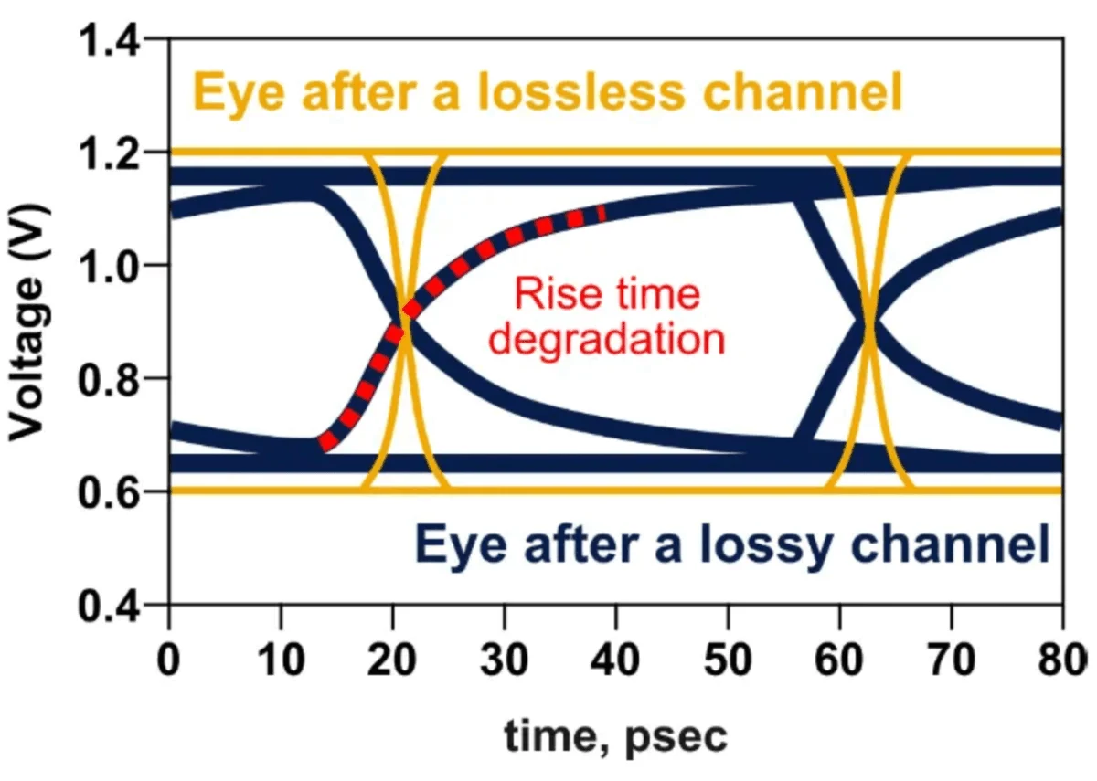
Furthermore, the "eye diagrams" used to measure signal quality frequently show significant degradation in chiplet interconnects. Lossy channels lead to rise time degradation and increased jitter, making it difficult to maintain the high data rates required by standards like UCIe (Universal Chiplet Interconnect Express) and BoW (Bunch of Wires). If these issues are discovered late in the design cycle—during the post-layout verification stage—the cost of a design respin can reach millions of dollars, not to mention the loss of market share due to delayed product launches.

Stakeholder Concerns: From Architects to Project Managers
The move to chiplets has expanded the circle of stakeholders who must worry about interconnect performance. Previously, interconnects were often treated as a secondary concern after logic design. In the multi-die era, the interconnect is the heart of the system.
System architects are now faced with the daunting task of "system partitioning." They must decide which functions go on which die and which packaging technology to use—silicon interposers, organic substrates, or silicon bridges—long before a physical layout exists. These decisions are often made in a "blind spot," where the risks are highest because the physical characteristics of the interconnects are unknown.
Project managers and business executives are equally concerned with the predictability of the design cycle. The complexity of 3D stacking means that traditional margins of error are no longer sufficient. Foundries and Outsourced Semiconductor Assembly and Test (OSAT) providers are also under pressure to provide accurate models to their customers. If a chiplet-based system fails to meet its performance targets due to interconnect bottlenecks, the blame is often shared across the supply chain, leading to strained partnerships and increased legal risks.

The Limitations of Traditional Verification Workflows
The current crisis in chiplet design is exacerbated by the deficiencies of traditional Electronic Design Automation (EDA) workflows. Historically, EDA tools have followed a linear, post-layout-driven approach. In this model, engineers perform full electromagnetic (EM) extractions only after the physical layout of the package is finalized.
This "wait and see" approach is no longer viable for several reasons:
- Computational Intensity: Full 3D EM extraction for a complex interposer with thousands of signals is computationally expensive and can take days or even weeks to complete.
- Late Discovery: If the EM simulation reveals a signal integrity failure, the layout must be revised, and the entire process starts over. This creates a "bottleneck" that prevents rapid iteration.
- Lack of Early-Stage Fidelity: Pre-layout methods used in the past often relied on simplified circuit models that lack the high-fidelity accuracy needed to predict link margins for high-speed D2D interfaces. These tools struggle to account for the complex physics of hatched grounds and 3D vias.
- Manual Data Integration: Traditional tools often operate in silos. The data from an interconnect simulation might not seamlessly integrate with the Physical Layer (PHY) compliance verification tools, forcing teams to manually transfer data, which increases the risk of human error.
Keysight’s 3D Interconnect Design Solution: A Shift-Left Approach
To address these systemic challenges, Keysight Technologies has introduced a next-generation design solution specifically tailored for 3D interconnects in advanced packages. The philosophy behind this solution is "Shift-Left"—moving critical verification and simulation tasks earlier in the design cycle to identify and mitigate risks before the layout stage.

Keysight’s solution focuses on three pillars:
- Predictive Modeling: By using advanced algorithms that can accurately simulate the effects of hatched ground planes and 3D structures without requiring a finished layout, designers can explore the "design space" more freely. This allows architects to test different partitioning strategies and packaging materials with high confidence in the eventual SI/PI outcomes.
- Rapid Design Space Exploration: The solution enables fast, accurate insights based on physical design parameters. Instead of waiting weeks for a full EM extraction, engineers can run "what-if" scenarios in a fraction of the time, optimizing the number of traces, via placements, and shielding strategies.
- Integrated PHY-Level Compliance: Keysight has bridged the gap between interconnect simulation and PHY verification. Their tools allow for seamless testing against industry standards like UCIe. This ensures that the D2D links will not only function but will also be fully compliant with the rigorous specifications required for interoperability in a multi-vendor chiplet ecosystem.
Broader Industry Implications and Analysis
The shift toward specialized 3D interconnect design tools represents a maturing of the chiplet ecosystem. As the industry moves away from the "trial and error" phase of multi-die integration, the focus is shifting toward standardization and predictability. The adoption of the UCIe standard is a testament to this, providing a common language for chiplets from different manufacturers to communicate.
However, the success of the chiplet model depends entirely on the industry’s ability to solve the interconnect problem. If the "interconnect tax"—the overhead in power, area, and latency required to link chiplets—becomes too high, the benefits of disaggregation will be neutralized. Therefore, the development of high-fidelity, early-stage simulation tools is not just a convenience for engineers; it is a structural requirement for the continued scaling of semiconductor performance.

In the long term, we can expect to see an even tighter integration between EDA software and manufacturing data. Foundries will likely provide more detailed "golden models" of their packaging processes that plug directly into tools like those offered by Keysight. This will create a "digital twin" of the advanced package, allowing for real-time optimization of signal and power integrity. As AI continues to drive the demand for more powerful silicon, the ability to master the third dimension of chip design—the 3D interconnect—will become the primary differentiator for semiconductor companies in the decade to reach.
