
The semiconductor industry has reached a fundamental crossroads where the historical reliance on transistor scaling, famously characterized by Moore’s Law, is no longer the sole engine of computational progress. As the physical and economic costs of shrinking transistors to the 3nm and 2nm nodes escalate, the focus of innovation has shifted from the silicon wafer to the package. This transition is being defined by a new architectural paradigm known as "3.5D integration," a hybrid methodology that combines the lateral connectivity of 2.5D packaging with the vertical density of 3D stacking. By defying the conventional logic of simple addition, the 3.5D equation provides a solution to the most pressing challenges in the artificial intelligence (AI) and high-performance computing (HPC) sectors: thermal management, interconnect latency, and manufacturing yield.
The Decoupling of Moore’s Law and the Rise of Heterogeneous Integration
For over five decades, the semiconductor roadmap was dictated by the ability to double transistor density approximately every two years. However, as gate lengths approach atomic scales, quantum tunneling and leakage current have introduced severe physical limitations. Simultaneously, the cost of designing a leading-edge System-on-Chip (SoC) has skyrocketed, with estimates suggesting that a 3nm design can cost upwards of $600 million.
In response, the industry has embraced heterogeneous integration—the practice of combining multiple smaller chips, or "chiplets," into a single package. This allows designers to use the most advanced (and expensive) process nodes only for critical compute cores, while utilizing more mature, cost-effective nodes for I/O, power management, and memory controllers. While this modularity began with Multi-Chip Modules (MCM), the demand for bandwidth eventually necessitated the move to 2.5D integration.
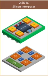
In a 2.5D configuration, multiple dies are placed side-by-side on a silicon interposer. This interposer acts as a high-density routing layer, providing significantly more connections than a traditional organic substrate. This technology became the industry standard for integrating High-Bandwidth Memory (HBM) with Graphics Processing Units (GPUs) and AI accelerators. However, as AI models grow in complexity, even the lateral bandwidth of 2.5D is becoming a bottleneck. The "reticle limit"—the maximum size a single lithography step can print—restricts the size of these interposers, forcing the industry to look upward.
A Chronology of Packaging Evolution: From 2D to 3.5D
The journey toward 3.5D integration is best understood through a timeline of packaging milestones that have addressed specific technological hurdles:
- 2010–2015: The 2.5D Breakthrough. The introduction of technologies like TSMC’s Chip-on-Wafer-on-Substrate (CoWoS) allowed for the first wide-scale integration of HBM. This era proved that lateral disaggregation could maintain performance while improving yield.
- 2016–2020: The 3D Stacking Era. Driven by the need for memory density, 3D NAND and later 3D logic stacking (such as Intel’s Foveros) emerged. By stacking dies vertically using Through-Silicon Vias (TSVs), designers achieved the shortest possible interconnect distances.
- 2021–Present: The 3.5D Synthesis. As AI workloads hit the "thermal wall," the industry realized that full 3D stacking of high-power logic was difficult to cool. 3.5D emerged as the pragmatic middle ground, selectively stacking only the most communication-intensive components while spreading others laterally to manage heat and cost.
This evolution represents a shift from a "chip-first" mentality to a "system-first" architecture, where the package is treated as an integral part of the silicon design rather than an afterthought.

The Technical Mechanics: Hybrid Bonding and Signal Density
The "3D" component of the 3.5D architecture relies on a revolutionary interconnect technology known as copper-to-copper hybrid bonding. Unlike traditional flip-chip packaging, which uses micro-bumps (small solder balls) to connect dies, hybrid bonding eliminates the bumps entirely. Instead, the copper pads of two chips are bonded directly together at the atomic level.
Data suggests that hybrid bonding enables signal densities approximately 7X to 10X higher than what is achievable with micro-bumps. Furthermore, because the interconnects are shorter and lack the parasitic capacitance of solder bumps, the interface power consumption is reduced by roughly 10X. This is critical for AI "XPUs" (GPUs, TPUs, and NPUs), where the energy required to move data between a processor and its memory often exceeds the energy required to perform the actual calculation.
In a 3.5D system, these vertically stacked units—perhaps a compute tile stacked directly on top of a cache layer—are then placed onto a 2.5D interposer alongside HBM modules and I/O chiplets. This creates a "cluster" of high-density vertical performance within a broader, manageable lateral framework.
The Thermal and Economic Imperative: Why 3.5D?
While full 3D stacking offers the best theoretical performance, it introduces two major risks: thermal throttling and yield loss. High-performance AI chips are now approaching kilowatt-scale power consumption. If two high-power logic dies are stacked directly on top of each other, the bottom die becomes insulated, leading to heat buildup that can degrade performance or cause permanent hardware failure.
3.5D integration mitigates this by allowing architects to be selective. Only components with lower power profiles or those that strictly require vertical proximity for latency reasons are stacked. The rest of the system is distributed across the 2.5D interposer, providing a larger surface area for heat sinks and liquid cooling solutions to operate effectively.
From an economic perspective, 3.5D addresses the "Known Good Die" (KGD) problem. In a complex 3D stack, if one die in a stack of four is defective, the entire stack—including the three functional dies—is often scrapped. By limiting the vertical stacks to fewer layers and integrating them into a 2.5D environment, manufacturers can maintain higher yields and lower the total cost of ownership for data center operators.
Industry Momentum and Stakeholder Reactions
The shift toward 3.5D is not merely theoretical; it is being driven by the largest players in the semiconductor ecosystem. Foundries like TSMC, Samsung, and Intel have all launched comprehensive 3D-IC platforms (such as TSMC’s 3DFabric) to support these hybrid designs.

EDA (Electronic Design Automation) providers are also pivotally involved. Companies like Cadence have released unified platforms, such as the Integrity 3D-IC Platform, to handle the "multiphysics" challenges of 3.5D. These tools allow designers to simulate electrical, thermal, and mechanical stresses simultaneously. Industry analysts note that without these advanced simulation capabilities, the risk of "package warpage" or timing failures in 3.5D designs would be too high for commercial viability.
Recent market activity highlights this trend. Broadcom’s recent shipment of custom AI silicon to Fujitsu, which utilizes 3.5D-style multi-tile architectures, serves as a benchmark for the industry. Hyperscalers like Google, Meta, and Amazon are also reportedly moving toward 3.5D for their in-house AI accelerators (TPUs and Trainium/Inferentia chips) to stay ahead of the massive computational requirements of Large Language Models (LLMs).
Broader Impact and the Future of AI Silicon
The implications of 3.5D integration extend far beyond the technical specifications of a single chip. It represents a democratization of high-performance silicon design. By using a 3.5D approach, smaller "challenger" companies can potentially compete with industry giants by intelligently architecting chiplet-based systems that perform like monolithic giants but cost significantly less to manufacture.
Furthermore, 3.5D is likely to be the primary enabler for the next generation of "AI Superchips." As the industry moves toward systems that require trillions of parameters to be processed in real-time, the ability to minimize the "memory wall" through vertical stacking while maintaining the modularity of 2.5D will be the deciding factor in who leads the AI arms race.
In conclusion, 3.5D integration is the architecture of practical innovation. It acknowledges that while vertical stacking is the future, the industry must remain grounded in the realities of thermodynamics and manufacturing economics. By combining the best of both worlds, 3.5D ensures that the trajectory of computational power continues to climb, even as the era of traditional transistor scaling begins to fade. For the engineers and architects building the backbone of the digital age, the equation 2.5D + 3D = 3.5D is no longer a mathematical curiosity—it is the roadmap for the next decade of progress.
