
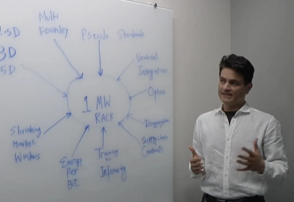
The rapid escalation of artificial intelligence capabilities is fundamentally reshaping the architecture of the modern data center, moving away from traditional general-purpose computing toward highly specialized, power-intensive environments. As organizations transition from basic machine learning models to massive Large Language Models (LLMs) and generative AI frameworks, the hardware required to sustain these workloads has undergone a radical transformation. This evolution is characterized by a shift from monolithic processor designs to sophisticated systems-on-chips (SoCs) housed in multi-dimensional packages, all interconnected through high-speed optical signaling and tiered memory structures. Manmeet Walia, director of product management for mixed-signal PHY IP at Synopsys, recently highlighted these unprecedented changes, noting that the demand for performance is driving a spike in power consumption that necessitates a complete rethink of the server rack’s internal anatomy.
The Architecture of Acceleration: Inside the AI Rack
At the heart of the next-generation AI server rack lies a complex ecosystem of silicon designed to handle the dual demands of training and inferencing. Unlike traditional servers that relied heavily on Central Processing Units (CPUs), modern AI racks are dominated by specialized accelerators, often in the form of Graphics Processing Units (GPUs) or Tensor Processing Units (TPUs). A single rack now frequently contains a half-dozen or more high-performance SoC components, each specifically tuned for the matrix multiplications and parallel processing tasks essential to AI.
These SoCs are no longer simple chips mounted on a motherboard. To overcome the physical limitations of silicon scaling, industry leaders have moved toward advanced packaging techniques. These include 2.5D, 3D, and even 3.5D Integrated Circuits (3D-ICs). By stacking dies vertically or placing them side-by-side on a silicon interposer, manufacturers can achieve significantly higher transistor density and shorter interconnect distances. This reduces latency and power loss, which are critical when managing the terabytes of data flowing through the system every second.
The Power Challenge: Efficiency vs. Performance
The surge in AI performance has come at a significant cost: a massive increase in power consumption. A decade ago, a standard data center rack might have consumed between 5 kW and 10 kW of power. Today, high-density AI racks are pushing toward 100 kW and beyond. This trajectory presents a dual challenge for engineers: how to deliver sufficient electricity to the rack and how to dissipate the resulting heat.
Data from the International Energy Agency (IEA) suggests that data centers globally consumed approximately 460 terawatt-hours (TWh) in 2022, a figure that could more than double by 2026. Within the rack, individual chips are now reaching Thermal Design Power (TDP) ratings of 700W to 1,000W. For instance, NVIDIA’s Blackwell B200 GPU is reported to require up to 1,200W of power. To manage this, the industry is transitioning from air cooling to liquid cooling solutions, including direct-to-chip cold plates and immersion cooling, where the entire server is submerged in a non-conductive fluid.
Chronology of AI Hardware Evolution
The path to the current AI server rack has been defined by several distinct eras of computing:

- The CPU Era (Pre-2012): Data centers were primarily built for web hosting and database management. Racks were filled with multi-core CPUs (Intel Xeon or AMD EPYC) that handled serialized tasks. AI was a niche academic pursuit.
- The GPU Explosion (2012–2018): Following the success of AlexNet in 2012, the industry realized that GPUs were exceptionally well-suited for neural network training. This led to the first dedicated AI clusters, though they still utilized standard PCIe interconnects.
- The Specialized SoC Era (2018–2022): Companies like Google, Amazon, and Meta began developing their own silicon (ASICs) to optimize specific AI workloads. This era saw the introduction of High Bandwidth Memory (HBM) to solve the "memory wall" problem.
- The Disaggregated and 3D Era (2023–Present): The current phase involves disaggregating memory and compute. The rack is treated as a single massive computer rather than a collection of individual servers. Advanced 3D packaging and optical interconnects have become the standard for flagship deployments.
Advanced Packaging and 3D-IC Integration
As Manmeet Walia noted, the move toward 3D-IC and 3.5D structures is a response to the slowing of Moore’s Law. In a 3D-IC configuration, memory is often stacked directly on top of the logic die using Through-Silicon Vias (TSVs). This allows for a massive increase in the number of connections between the processor and its memory, providing the bandwidth necessary for LLMs.
The "3.5D" designation often refers to a hybrid approach that combines 3D stacking with 2.5D interposers. This allows different types of chips—such as logic, memory, and I/O—to be manufactured on different process nodes and then integrated into a single package. For example, a 3nm logic chip might be paired with a 7nm I/O chiplet and several HBM3e stacks. This modular approach, often called "disaggregation," allows for better yields and lower costs while maintaining peak performance.
Connectivity: From Copper to Optics
One of the most significant shifts in the next-generation rack is the transition from electrical to optical signaling. As data rates exceed 112 Gbps and move toward 224 Gbps per lane, traditional copper wiring encounters severe physical limitations. Signal integrity degrades rapidly over short distances, and the power required to push electrons through copper at these speeds becomes prohibitive.
To solve this, the industry is adopting Co-Packaged Optics (CPO) and silicon photonics. By integrating optical engines directly onto the SoC package, data can be converted into light signals immediately. This allows for massive throughput between racks and across the data center with minimal latency and significantly lower power consumption. Synopsys and other IP providers are currently developing the mixed-signal PHY (Physical Layer) IP required to bridge the gap between digital logic and these high-speed optical interfaces.
Memory Tiering and Disaggregation
The hunger for data in AI training has exposed the limitations of traditional memory hierarchies. In a next-generation rack, memory is being disaggregated into tiered structures. At the top tier is HBM (High Bandwidth Memory), located directly on the GPU or SoC package to provide the fastest possible access. However, HBM is expensive and capacity-limited.
To address this, the industry is utilizing the Compute Express Link (CXL) protocol. CXL allows for "memory pooling," where a central reservoir of memory can be shared dynamically among various processors in the rack. This second tier of memory—often using DDR5—provides the capacity needed for massive datasets that cannot fit entirely within HBM. This tiered approach ensures that processors are never "starved" for data, which is a common bottleneck in AI training efficiency.
Industry Implications and Market Reactions
The shift toward these complex, integrated server racks has major implications for the semiconductor supply chain. System-on-chip design is no longer just about the silicon; it is about the entire system, including thermal management, power delivery, and high-speed interconnects.

Market analysts suggest that the AI infrastructure market is poised for sustained growth. According to Gartner, the market for AI chips is expected to reach $71 billion in 2024, a 25% increase from the previous year. This growth is driving a "gold rush" for advanced packaging capacity, with companies like TSMC and Intel investing billions in new facilities to support CoWoS (Chip on Wafer on Substrate) and other advanced assembly techniques.
Major cloud service providers (CSPs) have reacted by vertically integrating their hardware stacks. Microsoft’s Maia 100 and Amazon’s Trainium2 chips are examples of custom-built SoCs designed specifically to fit into these next-generation racks. By controlling the silicon, these companies can optimize the power and performance of their entire data center footprint, reducing their reliance on third-party vendors and lowering the total cost of ownership.
Analysis: The Future of the AI Data Center
The insights provided by Synopsys’ Manmeet Walia underscore a fundamental truth: the AI revolution is as much a hardware challenge as it is a software one. The next-generation AI server rack is a marvel of engineering that pushes the boundaries of physics. However, the sustainability of this growth remains a point of concern.
As power requirements climb, the industry must continue to innovate in energy efficiency. The move toward 3D-ICs and optical signaling is a step in the right direction, but it may not be enough to offset the sheer scale of compute demand. Future developments may include the adoption of backside power delivery—where power is routed through the back of the silicon wafer to reduce interference—and the exploration of new materials like gallium nitride (GaN) for more efficient power conversion within the rack.
In conclusion, the next-generation AI server rack is no longer a collection of discrete components but a highly integrated, multi-dimensional system. From the 3D-IC packaging of the SoCs to the optical interconnects and tiered memory structures, every element is being optimized for the singular goal of accelerating AI. As these technologies mature, they will define the next decade of computing, determining which companies lead the AI race and how the global digital infrastructure evolves to meet the needs of an AI-driven world.
