

The semiconductor industry is currently navigating a pivotal transition in its manufacturing paradigm, shifting from traditional geometric scaling to a complex, system-level optimization challenge defined by Edge Placement Error (EPE). This shift was the focal point of the recent SPIE Photomask Technology + Extreme Ultraviolet (EUV) Lithography conference, where industry leaders from IBM, Carl Zeiss SMT, Micron Technology, ASML, Tekscend, and Applied Materials convened to address the mounting pressures of device fabrication at the sub-3nm node. As features shrink, EPE—the difference between the intended design edge and the actual printed edge on a wafer—has evolved from a localized lithography metric into a comprehensive indicator of manufacturing health and device yield.
The conference underscored that the industry can no longer rely on isolated process optimizations. While individual modules such as mask fabrication, scanner performance, resist chemistry, and etch processes have historically been optimized in silos, this approach is reaching its mathematical limit. Experts at the SPIE event warned that a collection of locally optimized processes does not equate to a globally optimized device. Instead, EPE has emerged as a system-level phenomenon, where the cumulative impact of stochastic effects, pattern-dependent mask profiles, and process-induced stress necessitates a holistic, data-driven methodology.
Historical Evolution of the EPE Challenge
To understand the urgency of the current EPE discourse, one must look at the timeline of lithographic scaling. In the era of deep ultraviolet (DUV) lithography, EPE was primarily a function of overlay accuracy and critical dimension (CD) uniformity. However, as the industry transitioned to EUV, the introduction of high-numerical-aperture (High-NA) optics and complex multi-patterning techniques fundamentally changed the error budget.
By 2020, as nodes progressed toward 5nm and 3nm, the industry began observing that traditional Optical Proximity Correction (OPC)—the software-based process of modifying mask shapes to compensate for diffraction effects—was struggling to account for non-linear process interactions. Between 2022 and 2024, the industry saw a surge in research concerning stochastic variability, where random photon-counting effects and chemical fluctuations in photoresists began to dominate the EPE budget. The SPIE conference served as a bellwether, confirming that EPE is now the primary constraint preventing the continued shrinkage of pitch and feature size.
The Role of OPC: From Correction Tool to System Superhero
A central theme at the SPIE panel was the expanding scope of OPC. Industry polls conducted during the event revealed that a significant majority of participants—approximately 58 percent—view OPC as the primary mechanism for reducing EPE in future nodes. This places immense pressure on Electronic Design Automation (EDA) providers to elevate OPC from a geometric adjustment tool to a comprehensive predictive engine.
However, the consensus among panelists was that OPC cannot operate in a vacuum. As EPE becomes an "unbounded budget" problem—incorporating variables ranging from wafer-to-die bonding stress to mask three-dimensional (3D) effects—OPC tools require higher-fidelity input data. Currently, many OPC workflows rely on empirical tables or simplified "etch" terms to account for complex process interactions. While these methods are effective for throughput and scheduling, they lack the physical rigor required to solve the tighter tolerances of the 2nm node and beyond. Experts from Micron and Applied Materials emphasized that EDA must evolve to represent the manufacturing environment in its entirety, integrating pattern-dependent mask profiles and realistic metrology feedback loops.
Data Quality Over Data Quantity
A recurring misconception addressed by the panel was the belief that simply collecting more data would resolve EPE issues. In modern fabrication facilities, the sheer volume of data generated by Scanning Electron Microscopy (SEM) and other metrology tools is already overwhelming. The challenge lies in the "signal-to-noise" ratio of the data.

Future EPE reduction strategies must focus on "physically meaningful" data. This involves moving beyond simple CD extraction to analyzing full-contour profiles, sidewall angles, and local geometry context. By utilizing OPC models to identify hotspots—areas of the design most sensitive to process variation—fabs can direct their metrology resources more efficiently. This creates a closed-loop system: modeling identifies the high-sensitivity areas, metrology validates the models, and the resulting insights focus engineering efforts on the specific process steps that impact yield most significantly.
Integrating AI with Physics-Based Modeling
The integration of Artificial Intelligence (AI) into the EPE workflow is inevitable, yet it remains a point of contention regarding explainability. While machine learning (ML) models are highly adept at identifying systematic patterns that traditional physics-based models miss, the semiconductor industry requires a level of transparency that "black-box" AI cannot currently provide.
The panel proposed a hybrid framework: explainable AI anchored by rigorous simulation. In this model, AI serves as an optimization agent that suggests adjustments to mask geometry or scanner settings, but these suggestions must be bounded by known physical laws. The industry’s adoption of these agentic systems will likely follow a phased approach, starting with well-defined tasks such as global CDU (Critical Dimension Uniformity) reduction and source-mask optimization, before moving toward broader, autonomous process control.
Connecting Manufacturing to Product Performance
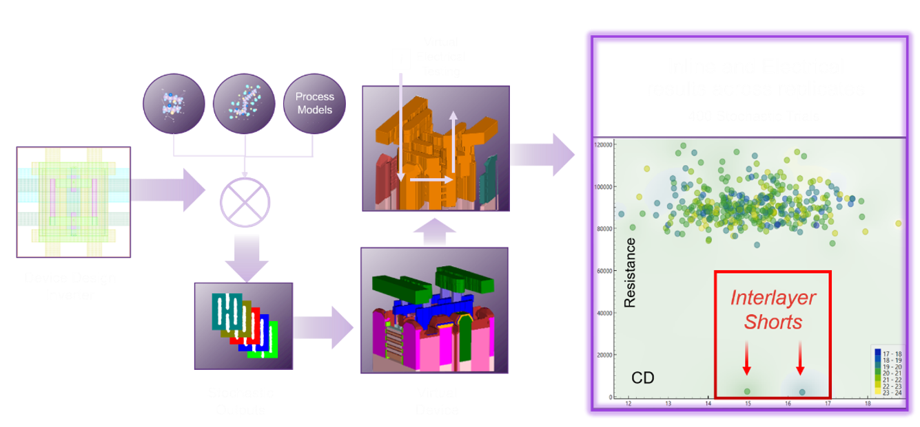
Perhaps the most significant shift discussed was the necessity of connecting EPE to the final "PPA-Y" (Power, Performance, Area, and Yield) metrics. EDA providers are being tasked with bridging the gap between geometric EPE and electrical reality. Not all edge placement errors are created equal; some geometric deviations are negligible, while others, even at the sub-nanometer scale, can cause fatal shorts or opens in the circuit.
By integrating electrical simulation with lithography and process modeling, EDA tools can shift the focus from "perfect geometry" to "optimal performance." This allows engineers to allocate the limited process margin where it matters most, ensuring that the most critical paths of a high-performance processor receive the highest level of correction, while less sensitive areas are optimized for throughput and cost.
Implications for the Semiconductor Ecosystem
The implications of this EPE-focused strategy are profound for foundries, IDMs, and the broader supply chain. The transition requires a departure from the traditional, siloed model of equipment manufacturing and design. Foundries, as the central hubs of the manufacturing flow, must drive deeper, more purposeful partnerships with EDA and metrology providers.
The industry is moving toward a future of "time-dependent, system-level optimization," where factors like wafer-to-die bonding and three-dimensional integration become standard considerations in the EPE budget. This era will likely last for decades, as the industry moves beyond planar scaling to 3D device architectures.
In conclusion, the SPIE conference clarified that the era of EPE is a long-term, systemic challenge that demands a unified industry response. The "superhero" burden placed on OPC is only sustainable if the entire ecosystem—from the mask house to the metrology bench—works to feed the models the information they need to succeed. The path forward for semiconductor scaling is not found in a single breakthrough, but in the connective intelligence provided by EDA, the rigor of physics-based modeling, and the strategic collaboration of every entity involved in the fabrication process. By transforming fragmented process knowledge into a cohesive, system-level intelligence, the industry can continue to deliver the performance gains that have defined the digital age for the last half-century.
