
The semiconductor industry is currently navigating a period of unprecedented architectural complexity. As System-on-Chip (SoC) designs transition toward 3nm and 2nm process nodes, incorporating billions of transistors and heterogeneous integration through chiplets, the traditional methods of ensuring chip health are proving insufficient. Historically, chipmakers relied on static characterization, post-production testing, and generous "guard-banding"—the practice of setting performance margins to account for potential degradation. However, in the era of hyperscale data centers, autonomous driving, and generative AI, these "set-and-forget" methodologies are being replaced by a more dynamic, continuous approach: hardware monitoring.
While the deployment of on-chip monitors and sensors is becoming a standard requirement, a critical gap has emerged in the implementation phase. Industry experts and hardware engineers are increasingly recognizing that sensors alone cannot solve the visibility challenge. Without a robust, unified hardware monitoring infrastructure to orchestrate data, the resulting telemetry is often fragmented, difficult to integrate, and impossible to scale. The shift from simple sensing to comprehensive infrastructure represents a fundamental evolution in Silicon Lifecycle Management (SLM), providing a bridge between raw silicon data and actionable operational insights.
The Evolution of Semiconductor Complexity and the Monitoring Mandate
The drive toward advanced process technologies like Gate-All-Around (GAA) FETs and Backside Power Delivery (BSP) has significantly narrowed the margins for error. Modern SoCs feature dozens of power domains and complex clocking schemes that are highly sensitive to environmental fluctuations. Factors such as local IR drop (voltage sag), thermal hotspots, and aging-induced timing degradation can lead to "silent data errors"—faults that occur during operation without triggering a traditional system crash, leading to corrupted data and unreliable AI model outputs.
Data from recent industry studies suggests that as chips scale, the probability of latent defects—faults that pass initial production tests but manifest during the first year of field operation—has risen by nearly 30% in advanced nodes. This has forced a shift in the industry’s chronology of quality assurance. Previously, the lifecycle was bifurcated into "Test" (at the factory) and "Operation" (in the field). Today, these phases are merging into a continuous loop of monitoring that spans from initial silicon bring-up through the entire functional life of the device.
The Infrastructure Gap: Why Sensors Alone Are Insufficient
The primary challenge facing chip designers is not the lack of sensors, but the difficulty of integrating them into a coherent system. When sensors are treated as isolated IP blocks, engineering teams face significant hurdles. These include the manual effort required to route signals across a massive die, the lack of standardized interfaces for data retrieval, and the high computational overhead required if raw data must be processed by the main CPU.
Without a dedicated infrastructure, the "data tax" of monitoring can become prohibitive. Streaming raw measurements from thousands of on-chip points consumes valuable interconnect bandwidth and power. Furthermore, if the monitoring logic is not unified, the software stack used during production testing often cannot be reused when the chip is deployed in a server or a vehicle. This fragmentation leads to extended development cycles and increased risk, as the monitoring solution may fail to provide real-time alerts when they are most needed.

A Unified Architecture for Hardware Monitoring
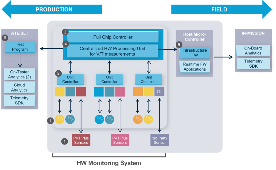
To address these challenges, proteanTecs has introduced a five-layer hardware monitoring infrastructure designed to provide a "smart control architecture." This system connects on-chip "Agents" (deep data generators) to both factory test equipment and in-field software through a single, reusable framework.
The architecture is structured to handle the entire data pipeline. At the base layer (Layer 1) are the Agents and PVT (Process, Voltage, Temperature) sensors that sit within the silicon. Layers 2 through 4 constitute the core infrastructure, managing the orchestration, data processing, and unified control. Layer 5 consists of the applications—such as analytics platforms or firmware—that consume the processed data.
The innovation of this approach lies in its "integrate once, deploy anywhere" philosophy. By using standard industry interfaces (such as JTAG, I2C, or SPMI), the infrastructure allows the same monitoring logic used by a test engineer in the lab to be accessed by a system administrator in a remote data center. This continuity ensures that the performance baselines established during production remain valid throughout the chip’s life.
Real-Time Hardware Processing and Bandwidth Optimization
A key feature of modern monitoring infrastructure is the ability to process data directly on-chip. Rather than acting as a passive conduit for raw numbers, the infrastructure includes embedded controllers that perform statistical analysis and threshold monitoring in hardware.
This "edge computing for silicon" provides two major advantages. First, it drastically reduces bandwidth requirements. Instead of continuously streaming voltage readings, the system only transmits a signal when a specific "droop" threshold is crossed or when a statistical anomaly is detected. Second, it enables a real-time response. In mission-critical applications, such as an autonomous vehicle’s ADAS (Advanced Driver Assistance System), waiting for a software loop to process a thermal spike could be catastrophic. Hardware-based alerts trigger immediately, allowing the system to throttle performance or switch to a redundant path within microseconds.
Deep Data Generators: The Role of Agents and PVT Sensors
The effectiveness of any monitoring system is ultimately determined by the quality of the data it collects. The proteanTecs system utilizes two primary categories of generators:
- On-Chip Agents: These are high-resolution IP blocks that measure complex parametric data. Unlike simple sensors, Agents can observe timing margins, cycle-to-cycle jitter, and process signatures. They are strategically embedded into the design to monitor "at-risk" paths, providing a high-fidelity map of the chip’s internal health.
- PVT Sensors: Specifically designed for advanced nodes (GAA and BSP), these sensors manage the "operational environment." They track voltage droops and thermal gradients with high precision, which is essential for managing the power-dense environments found in modern AI accelerators.
By mixing and matching these Agents based on the specific needs of the block—whether it is a high-speed SerDes interface or a dense memory array—chipmakers can tailor their visibility without changing the underlying infrastructure.

Automation and the EDA Integration Flow
One of the most significant barriers to adopting comprehensive monitoring has been the implementation effort. To mitigate this, the industry is moving toward automated generation of monitoring subsystems. ProteanTecs’ EDA (Electronic Design Automation) tools now include compilers that automatically generate the hardware monitoring system, including the necessary firmware and verification collateral.
This "compiler-driven" approach allows designers to integrate the system with minimal impact on the physical layout. The system typically operates on low-frequency interface signals and does not require internal memory resources, making it "agnostic" to the primary chip architecture. This ease of integration is crucial for maintaining time-to-market schedules in the competitive semiconductor landscape.
Industry Implications and the Path to 2nm
The broader impact of comprehensive hardware monitoring extends beyond simple maintenance. For hyperscalers like Google, AWS, and Meta, the ability to predict a chip failure before it occurs can save millions of dollars in avoided downtime. In the automotive sector, where the ISO 26262 standard mandates rigorous safety and reliability, continuous monitoring provides the "digital twin" of the hardware necessary for long-term compliance.
As the industry moves toward 2nm, the physics of silicon become increasingly volatile. At these scales, "aging" (the gradual degradation of transistors) happens faster and more unpredictably. A unified hardware monitoring infrastructure is no longer a luxury but a fundamental requirement for the viability of next-generation electronics.
Chronology of Semiconductor Quality Assurance
- 1990s – Early 2000s: Focus on "Design for Test" (DFT) and Scan chains. Quality was determined almost entirely at the factory gate.
- 2010s: Rise of In-System Test (IST) and basic thermal throttling. High-end chips begin to include simple sensors for self-protection.
- 2020 – 2023: Emergence of Silicon Lifecycle Management (SLM). The industry recognizes the need for data collection post-deployment.
- 2024 and Beyond: The shift to Unified Monitoring Infrastructure. Monitoring becomes an integral, automated part of the SoC architecture, providing real-time telemetry from production to end-of-life.
Conclusion: The Strategic Value of a Complete System
Chipmakers today face a choice: they can attempt to stitch together disparate sensors and proprietary logic, or they can adopt a proven, end-to-end monitoring system. The latter, exemplified by the proteanTecs platform—which has been implemented in over 150 designs across all major foundries—offers a lower-risk path to market.
By providing a single infrastructure that supports both production test and mission-mode operation, proteanTecs has eliminated the "missing pieces" of the monitoring puzzle. As SoCs continue to scale in complexity, the value of this visibility will only grow, serving as the definitive safeguard for the performance, quality, and reliability of the global silicon supply chain. For companies looking to maintain a competitive edge in the 2nm era, the transition from "sensing" to "comprehensive infrastructure" is the next logical—and necessary—step.
