
The semiconductor industry is currently navigating one of its most significant architectural shifts in decades as logic devices transition from FinFET (Fin Field-Effect Transistor) structures to the more complex Gate-All-Around (GAA) architectures. While GAA technology, often referred to as nanosheet or multibridge-channel FETs, offers superior electrostatic control and scaling potential, it has introduced unprecedented manufacturing challenges. Specifically, manufacturing variability has emerged as a primary barrier to achieving commercially viable high yields. To address this, Lam Research has unveiled a groundbreaking digital twin-driven yield optimization methodology that utilizes virtual fabrication and machine learning to explore process variations, reduce failure rates, and drastically accelerate the development cycle of advanced logic nodes.
The Strategic Shift from FinFET to Gate-All-Around
For the past decade, FinFET technology has been the workhorse of the semiconductor industry, powering multiple generations of high-performance computing and mobile devices. However, as the industry pushes toward the 3nm node and beyond, the physical limitations of FinFETs—such as short-channel effects and sub-threshold leakage—have become increasingly difficult to manage. GAA architectures solve these issues by surrounding the channel on all four sides with the gate material, allowing for better drive current and reduced power consumption.
Despite these benefits, the transition to GAA is fraught with manufacturing complexity. The shift involves moving from a 2D-like fin structure to a 3D stack of nanosheets. This transition requires hundreds of tightly coupled process steps, including the deposition of alternating layers of silicon and silicon-germanium, selective etching of sacrificial layers, and the formation of internal spacers. In such an environment, traditional wafer-based optimization—which relies on physical "trial and error" in a cleanroom—is proving to be prohibitively slow and expensive. A single experimental cycle can take months, and with the cost of a leading-edge wafer run exceeding tens of thousands of dollars, the industry has reached a tipping point where virtual solutions are no longer optional but essential.
Implementing the Full-Flow Digital Twin
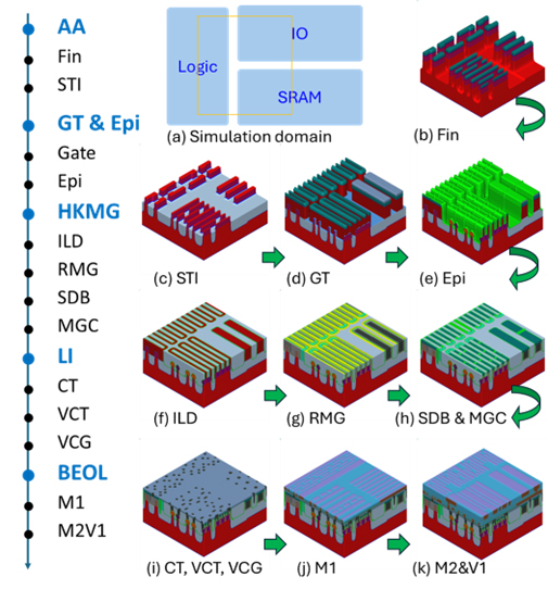
Lam Research’s solution centers on the creation of a full-flow digital twin of the GAA logic fabrication process. Unlike traditional simulations that focus on isolated steps, this digital twin faithfully reproduces the entire manufacturing sequence within a single simulation domain. This includes the Front-End-of-Line (FEOL), Middle-of-Line (MOL), and Back-End-of-Line (BEOL) steps.
The simulation domain is comprehensive, covering critical regions such as Static Random-Access Memory (SRAM), standard logic, and Input/Output (I/O) structures. By modeling these in sequence, engineers can observe how a variation in an early step—such as fin formation—ripples through the process to affect the final metallization. Key modules integrated into the workflow include:
- Fin Formation and Isolation: Modeling the initial shaping of the transistor structure and the implementation of Shallow Trench Isolation (STI).
- Dummy Gate and Internal Spacer Processing: Simulating the complex removal of sacrificial materials and the delicate placement of spacers that define the gate length.
- Source/Drain Epitaxy (EPI): Monitoring the crystalline growth of materials that form the transistor’s terminals, a frequent source of defects.
- Replacement Metal Gate (RMG) Formation: The critical step of filling the gate cavity with high-k dielectrics and metal work-function layers.
- Self-Aligned Contacts and BEOL Metallization: Ensuring that the electrical connections to the transistor are perfectly aligned and free of shorts.
Identifying and Visualizing Failure Modes
One of the primary advantages of the digital twin approach is the ability to make failure modes visible long before a physical wafer is even processed. In the GAA workflow, Lam Research identified and defined more than 10 common failure modes that frequently plague advanced logic development.
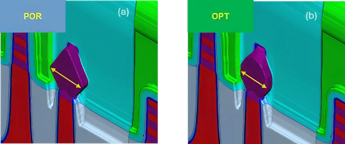
Through high-resolution virtual modeling, engineers can pinpoint the exact physical location and cause of defects. Representative examples include fin top damage during etching, poly gate residue that leads to electrical leakage, and "EPI mushroom" defects where epitaxy growth exceeds its intended boundaries, causing structural collapse. Perhaps most critically, the digital twin allows for the study of Source/Drain-to-Metal-Gate (SD-to-MG) shorts and EPI-to-EPI shorts, which are among the most difficult defects to diagnose in a physical fab environment due to their sub-surface nature.

By categorizing these defects virtually, the methodology moves from reactive troubleshooting to proactive prevention. Engineers can visualize the "process window"—the range of parameters within which a device will function correctly—and understand which specific steps are most likely to push the process out of that window.
Machine Learning: The Engine of Optimization
The integration of machine learning (ML) marks a departure from traditional statistical process control. In Lam’s methodology, key process parameters are statistically varied around baseline conditions to simulate the natural "drift" and variability found in real-world manufacturing tools. The ML optimization engine then analyzes the resulting data to evaluate failure ratios across all modes simultaneously.
Rather than optimizing for one defect at a time—which often inadvertently worsens another defect—the ML engine retargets inline metrology specifications to minimize the total failure rate. This holistic approach is crucial for GAA, where the trade-offs between different process steps are highly non-linear.
The results of this ML-driven optimization are statistically significant. In a baseline scenario (Process of Record, or POR), the overall pass ratio for the simulated GAA structure was a mere 1.6%, a figure that would render any commercial fab insolvent. However, after the ML engine optimized the parameters:

- SD-to-MG shorts were reduced from approximately 80% to near zero.
- N/P EPI shorts dropped from roughly 69% to approximately 4%.
- Source/Drain opens (lack of electrical contact) were nearly eliminated.
The cumulative effect of these improvements was a surge in the overall pass ratio from 1.6% to 87.2%. This 50-fold increase in yield potential demonstrates the power of shifting experimentation from the physical to the virtual realm.
Translating Virtual Insights into Actionable Metrology
For a digital twin to be effective, its insights must be translatable into the physical factory floor. Lam’s methodology achieves this by producing actionable metrology targets. For example, the simulation might reveal that reducing epitaxy growth time and adjusting the size of the EPI region can mitigate the risk of EPI-to-EPI shorts.
The digital twin provides specific, numerical targets for hundreds of parameters that fab engineers can program into their lithography, etch, and deposition tools. This "virtual-to-physical" bridge ensures that the optimized process window discovered in the simulation is maintained during actual high-volume manufacturing. This capability is expected to significantly reduce the "cycle time of learning," which is the time it takes for a fab to identify a problem, test a solution, and implement it.
Chronology and Timeline of Development
The development of this digital twin methodology follows a multi-year trajectory of innovation within the semiconductor equipment sector.
- 2020–2022: Initial industry research focused on the feasibility of GAA (nanosheet) scaling and the identification of atomic-level channel challenges.
- 2023: Early integration of human-machine collaboration in process development, as highlighted in joint studies by researchers at Lam and various academic institutions.
- 2024–2025: The refinement of "Semiverse Solutions," Lam’s suite of virtual fabrication tools, which moved from simulating individual tool performance to simulating entire process flows.
- 2026 and Beyond: The current phase, where digital twins are being used as a standard "pre-flight" check before physical wafers are committed to the line, specifically for 2nm and 1.4nm pilot production.
Industry Implications and Expert Perspectives
The implications of this technology reach far beyond the walls of Lam Research. Industry analysts suggest that the ability to simulate yield could be the deciding factor in which chipmakers win the race to the 2nm node. Foundry giants such as TSMC, Samsung, and Intel are currently investing billions in GAA technology, and any tool that can reduce the time-to-market for these nodes is worth its weight in gold.
"The economics of semiconductor scaling have changed," notes one industry analyst specializing in advanced technology nodes. "We can no longer afford to ‘build it and see.’ The cost of failure is too high. Digital twin technology provides a safety net that allows for aggressive innovation without the risk of catastrophic yield loss."
Furthermore, this methodology supports the broader industry trend of "Shift Left," where design and manufacturing concerns are addressed earlier in the product lifecycle. By identifying yield-killing defects in the virtual stage, companies can adjust their designs or process flows before they become ingrained in the manufacturing infrastructure.
Conclusion: A Scalable Path Forward
The study presented by Lam Research demonstrates that digital twin technology, when combined with the analytical power of machine learning, can fundamentally transform the semiconductor manufacturing landscape. By shifting the burden of experimentation to a virtual environment, the industry can overcome the inherent complexities of Gate-All-Around logic.

This methodology not only reduces development costs and shortens cycle times but also provides a scalable framework for future nodes. As device architectures continue to evolve toward even more exotic structures—such as Complementary FETs (CFETs) or 3D-stacked logic—the role of the digital twin will only become more central. For now, the transition to GAA serves as the ultimate proving ground for this technology, offering a clear and efficient path toward the next generation of high-performance computing.
