
The semiconductor industry is currently navigating a pivotal transition as Dynamic Random Access Memory (DRAM) technologies scale toward increasingly tighter pitches, pushing the physical boundaries of conventional lithography. As manufacturers move into advanced nodes such as D1b (1-beta), active-area (AA) pitches have contracted to a range between 22 and 26 nm. This dimension is significantly below the resolution capabilities of single-exposure Deep Ultraviolet (DUV) lithography, necessitating a shift toward sophisticated multi-patterning strategies. Among these, Self-Aligned Quadruple Patterning (SAQP) has emerged as a cornerstone technique to achieve sub-lithographic dimensions. However, the complexity of SAQP introduces new manufacturing vulnerabilities, specifically pitch walk and line-edge roughness (LER), which can jeopardize device yield. To address these challenges, engineers at Lam Research’s Semiverse Solutions have turned to Monte Carlo virtual fabrication to define safer process windows and prevent the costly failure of physical wafer experiments.
The Evolution of DRAM Patterning and the Scaling Wall
The roadmap for DRAM density has historically relied on the steady reduction of the "pitch"—the distance between identical features on a chip. For decades, DUV lithography was sufficient to meet these requirements. However, the Rayleigh criterion, which defines the resolution limit of optical systems, has finally caught up with memory production. At the 1-beta node, the required feature sizes are so small that a single light exposure can no longer resolve the individual lines of the active area.

To circumvent this, the industry adopted Self-Aligned Double Patterning (SADP) and, subsequently, Self-Aligned Quadruple Patterning (SAQP). SAQP is essentially a pitch-multiplication process. It begins with a lithography-defined "mandrel" and uses two successive cycles of spacer deposition and etching to create four features for every one mandrel originally printed. While theoretically elegant, this multi-step flow is highly sensitive. Small variations in the initial mandrel width, the conformality of the deposited layers, or the precision of the etch steps can be amplified. This amplification leads to "pitch walk"—a phenomenon where the spacing between lines becomes uneven, alternating between being too wide and too narrow.
The Mechanics of SAQP and the Genesis of Pitch Walk
The full process sequence of DRAM patterning in an SAQP flow is a rigorous exercise in material science and plasma physics. It begins with the formation of primary mandrels. A spacer material is deposited over these mandrels, followed by an anisotropic "spacer etch" that leaves material only on the sidewalls. The original mandrels are then removed, leaving behind a set of "second-generation" mandrels. This process is repeated a second time.
Ideally, this sequence results in four perfectly equidistant lines and trenches. In a high-volume manufacturing environment, however, perfection is elusive. Pitch walk is the primary byproduct of non-periodicity in this sequence. If the first spacer is slightly too thick, or the second etch is slightly too aggressive, the resulting trenches will not be uniform. This misalignment is more than a geometric nuisance; it can cause critical failures in the alignment of wordlines (WL), bitlines (BL), and contacts, effectively rendering the memory cell non-functional.

Furthermore, the industry must contend with Line Edge Roughness (LER). LER is driven by stochastic effects—random variations in photon flux (shot noise) and the diffusion of acids during the lithographic chemically amplified resist process. When the geometric errors of pitch walk collide with the jagged edges of LER, the "process window" (the range of parameters where the chip works) collapses. The result is a line-bridge defect, where two adjacent lines touch, creating an electrical short.
Methodology: Virtual Fabrication and Monte Carlo Analysis
To navigate this complex landscape without the prohibitive expense of processing hundreds of physical "short-loop" wafers, the Semiverse Solutions team utilized SEMulator3D for virtual fabrication. This environment allows engineers to build a digital twin of the fabrication process, incorporating real-world physical variables.
The study focused on several key input parameters known to influence pitch walk:

- Isotropy1 and Isotropy2: These represent the etch characteristics of various layers, including the Dielectric Anti-Reflective Coating (DARC) and the spacers. Isotropy measures how much a process etches sideways versus downwards.
- Deposition Conformality: This controls how evenly the spacer material covers the sidewalls of the mandrels.
- Lithography Variation: This accounts for focus and exposure fluctuations that impact the initial critical dimension (CD) of the printed mandrel.
- LER Amplitude: A representation of the stochastic roughness of the lines.
In this virtual model, the initial print CD was set to 60 nm, with the goal of achieving final line and trench CDs of 15 nm. The success criterion for the process was a pitch walk limit of 7.5 nm. By using Monte Carlo simulations—a mathematical technique that runs thousands of trials with randomized inputs based on probability distributions—the team could observe how these variables interacted in a way that isolated testing could never reveal.
Analyzing the Data: Success Rates and Parameter Sensitivity
The baseline for the study was the "Process of Record" (POR), representing standard manufacturing conditions. The virtual metrology steps tracked three specific trench dimensions (labeled $alpha$, $beta$, and $gamma$) to calculate the pitch walk. The simulation identified that even-numbered trenches were the most susceptible to line-bridge defects, as the cumulative errors of the spacer flows tended to converge at these locations.
The results of the Monte Carlo Design of Experiments (DOE) provided a clear map of the manufacturing "safe zones."

- Pitch Walk Success Rate: The study found that under standard POR conditions, the success rate for staying within the 7.5 nm pitch walk limit was not guaranteed. However, by optimizing the standard deviation of specific parameters, the team identified a process window that yielded a maximum success rate of 83.89%.
- The Power of Interaction: One of the most significant findings was that defects often occurred even when individual parameters were within their allowed limits. For example, a slightly high etch isotropy combined with a minor lithography bias could trigger a line-merge defect, even if neither variation was "failing" on its own.
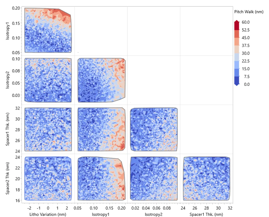
- Sensitivity Mapping: The team generated a contour plot matrix that served as a sensitivity map. It revealed that pitch walk is extremely sensitive to the interaction between "Isotropy1" and lithographic CD bias. If a fab cannot tighten its lithography control, it must compensate by significantly reducing etch isotropy to maintain the pitch walk specification.
The Physical Consequences of LER and Pitch Walk Interaction
The study also visualized the physical manifestation of these errors. At a low LER of 0.5 nm and a minimal pitch walk of 1.6 nm, the lines remained distinct. However, the tolerance for pitch walk drops precipitously as LER increases.
The simulations demonstrated that when LER reaches 1.5 nm, even a relatively "good" pitch walk can still result in a bridge defect. Conversely, if pitch walk reaches 6.6 nm, even a very "smooth" line (low LER) will likely merge with its neighbor. This interdependence highlights why advanced DRAM nodes require a holistic approach to process control rather than optimizing etch, deposition, and lithography in silos.
Industry Implications and Future Outlook
The implications of this study for the semiconductor industry are profound. As DRAM manufacturers like Samsung, SK Hynix, and Micron race to move beyond the 1-beta node toward 1-gamma and eventually sub-10nm nodes, the cost of research and development is skyrocketing. A single experimental wafer lot in a modern 300mm fab can cost tens of thousands of dollars and take weeks to process through the line.

Virtual fabrication offers a "fail fast" environment. By identifying that a specific combination of spacer thickness and etch isotropy will lead to an 18% failure rate before a single wafer is even loaded into a tool, companies can save millions in R&D costs and accelerate their time-to-market.
Furthermore, while this study specifically examined DRAM active-area patterning, the methodology is directly applicable to logic devices, such as Gate-All-Around (GAA) FETs, where multi-patterning and spacer-defined dimensions are equally critical. As the industry looks toward the adoption of High-NA EUV (Extreme Ultraviolet) lithography, virtual fabrication will likely remain an essential tool for hybrid patterning schemes where EUV is used in conjunction with self-aligned processes.
Conclusion
The transition to sub-26 nm pitches in DRAM has transformed patterning from a lithographic challenge into a multi-dimensional integration puzzle. The work performed by the Semiverse Solutions team at Lam Research underscores that "pitch walk" is the defining hurdle of the SAQP era. By leveraging Monte Carlo virtual fabrication, the industry now has a predictive roadmap to navigate this complexity.

The ability to quantify the interaction between stochastic LER and systematic process variations allows engineers to define a robust process window that ensures high yield. As semiconductor scaling continues to face the headwinds of physics, the integration of digital twins and statistical modeling into the fab workflow is no longer an optional luxury—it is a fundamental requirement for the next generation of memory technology. Through these advanced simulations, the path to the 1-gamma node and beyond becomes clearer, ensuring that the relentless pace of Moore’s Law continues in the memory sector.
