
The relentless progression of semiconductor scaling toward the sub-5nm regime has transformed minor layout nonuniformities from negligible anomalies into critical determinants of process success. In modern integrated circuit fabrication, a single chip layout comprises a complex mosaic of dense transistor regions, expansive open areas, and isolated functional features. This geometric heterogeneity presents a significant challenge for plasma etch processes, which encounter vastly different "local environments" across the surface of a 300mm silicon wafer. Even when utilizing a standardized process recipe, these environmental discrepancies manifest as pattern-dependent variation, where the etch rate and profile are dictated by the proximity and density of surrounding shapes.
The Technical Architecture of Pattern-Dependent Variation
Pattern-dependent variation is defined by the phenomenon where identical manufacturing parameters yield divergent physical results based on the local layout topography. To understand the gravity of this issue, one must examine the role of Shallow Trench Isolation (STI). STI is a critical fabrication step involving the etching of trenches to separate neighboring transistors, ensuring they do not suffer from electrical interference or "crosstalk." When the depth of these trenches varies—a condition known as recess nonuniformity—it creates a cascade of downstream manufacturing failures.

If an STI trench is etched too deeply or inconsistently across a die, the subsequent layers of film deposition and chemical mechanical planarization (CMP) will fail to achieve a flat profile. This lack of planarity prevents later lithographic steps from focusing correctly and causes electrical performance degradation in the final device. Consequently, STI recess variation is not merely an isolated manufacturing defect; it is a fundamental quality bottleneck that influences the entire process margin.
The root causes of this variation are primarily driven by two physical phenomena: Loading Effects and Aspect Ratio Dependent Etching (ARDE). Loading effects occur when the local concentration of reactive etchant species is depleted more rapidly in areas with a high density of material to be removed. Conversely, open regions with less material maintain a higher concentration of reactants, leading to a faster etch rate. ARDE, often referred to as "micro-loading" or "trenching," describes the difficulty of transporting reactants and removing byproducts within deep, narrow features. As the aspect ratio (depth-to-width) of a feature increases, the physical transport of ions and neutral species becomes restricted, causing narrower trenches to etch more slowly than wider ones. Together, these effects create a landscape of unpredictable depth variations across the wafer.
Historical Context and the Evolution of Layout Compensation
The challenge of pattern-dependent variation is not entirely new to the semiconductor industry, but its complexity has scaled exponentially with the move from planar transistors to 3D architectures like FinFETs and Gate-All-Around (GAA) nanosheets. In the 1990s and early 2000s, layout compensation was primarily focused on Chemical Mechanical Planarization (CMP). Engineers introduced "dummy fill"—non-functional geometric shapes—to balance the density of metal layers, ensuring that the polishing pads did not "dish" into large open areas.

As the industry moved toward the 22nm node and beyond, it became clear that etch processes were becoming just as sensitive to density as CMP. The industry transitioned from simple rule-based dummy fill to more sophisticated model-based approaches. However, the traditional method of verifying these layout changes involves "taping out" a new reticle (photomask), which can cost millions of dollars and take weeks to manufacture and test in a physical fabrication plant (fab). This high cost of experimentation has necessitated a shift toward "virtual fabrication" and advanced 3D process simulation to predict outcomes before a single wafer is processed.
Simulation Framework: Testing Dummy Fill Efficacy
To address the inefficiencies of physical trial-and-error, recent research has leveraged high-fidelity 3D process simulation tools, such as SEMulator3D, to create a digital twin of the manufacturing environment. By simulating the etch process on a virtual wafer, engineers can compare a "Process of Record" (POR) baseline against various layout modifications in a fraction of the time required for physical testing.
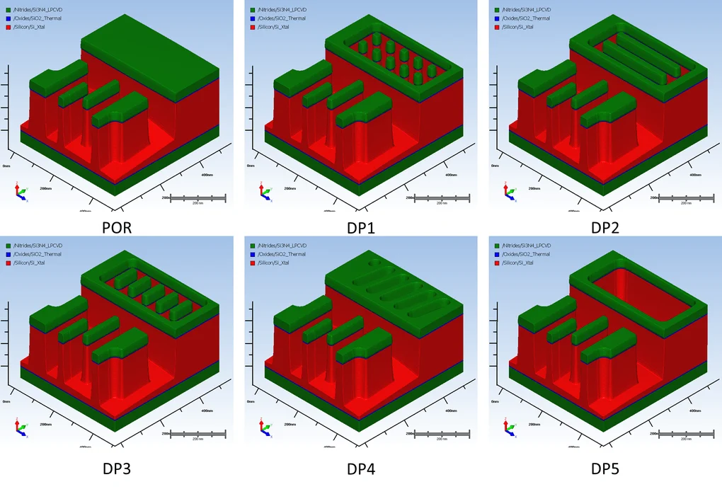
In a recent comprehensive study, researchers utilized a representative Static Random-Access Memory (SRAM) circuit layout to serve as the baseline. SRAM was selected due to its inherent asymmetry and its mix of repeating and non-repeating features, which provide a rigorous "stress test" for uniformity metrics. The study aimed to determine if trench depth could be stabilized across different neighborhoods, even when the critical dimension (CD) or linewidth remained constant.

The baseline analysis of the POR layout revealed a significant recess standard deviation of 8.2 nm across nine sampled locations. This variance was observed even in locations sharing the same CD, proving that the surrounding environment, rather than the feature size alone, was the dominant driver of etch depth. To mitigate this, the researchers designed five distinct dummy fill geometries to be integrated into the peripheral regions of the SRAM layout:
- Square Patterns: Standard blocks of non-functional material.
- Rectangular Patterns: Elongated shapes designed to mimic local wire traces.
- Circular Patterns: Geometries intended to minimize sharp corners and localized electric field concentrations.
- Ring-Shaped Patterns: Hollowed geometries to increase surface area without occupying excessive volume.
- Cross-Shaped Patterns: Complex geometries designed to balance density in multiple axes.
Quantitative Analysis of Dummy Open Density
The study introduced a critical metric known as "dummy open density" to evaluate the effectiveness of these shapes. Dummy open density represents the percentage of the dummy patterning area that has been removed via etching. For instance, a layout where 30% of the designated dummy area is etched away is assigned an open density of 30%.
The simulation results yielded a clear correlation: as the dummy open density increased, the recess standard deviation decreased. By removing more material in the dummy regions, the layout contrast—the difference between dense functional areas and open peripheral areas—was effectively neutralized. This "homogenization" of the layout allowed the plasma etch chemistry to behave more consistently across the die, as the reactive species were consumed at a more uniform rate.

While the data indicated that higher open density generally improved uniformity for this specific SRAM layout, researchers cautioned against viewing this as a universal law. The efficacy of dummy fill is highly dependent on the specific etch chemistry (e.g., halogen-based vs. fluorocarbon-based plasmas) and the specific process window of the equipment. However, the simulation successfully demonstrated that peripheral dummy fill could weaken the localized loading and ARDE effects that previously plagued the POR layout.
Industry Implications and Official Perspectives
The move toward simulation-based layout optimization reflects a broader industry trend known as Design-Technology Co-Optimization (DTCO). Major EDA (Electronic Design Automation) providers and semiconductor equipment manufacturers, such as Lam Research and Synopsys, have increasingly advocated for integrating process awareness into the early stages of chip design.
Industry analysts suggest that the ability to perform these simulations "off-fab" provides a massive competitive advantage. "In the current market, the difference between a successful product launch and a failure often comes down to yield ramp-to-market," noted a senior process integration engineer in a recent industry forum. "By using 3D simulation to finalize dummy fill strategies, we can skip two or three iterations of physical reticle updates. That represents a savings of both millions of dollars and months of development time."

Furthermore, the implementation of dummy fill is not without its trade-offs. Excessive dummy fill can introduce parasitic capacitance, which may slow down the switching speed of transistors or increase power consumption. Therefore, the goal of simulation is not just to improve etch uniformity, but to find the "Goldilocks zone" where process variation is minimized without compromising the electrical integrity of the circuit.
Broader Impact on the Future of Nanofabrication
As the semiconductor industry prepares for the transition to High-NA (Numerical Aperture) EUV lithography and the integration of backside power delivery networks, the role of pattern-dependent variation will only intensify. Future nodes will likely require "smart" dummy fills that are not only density-aware but also orientation-aware to account for the vectorial effects of advanced plasma sources.
The success of simulation-driven feedback loops, as demonstrated in the STI recess study, provides a blueprint for managing these complexities. By shifting the burden of process characterization from the physical fab to the digital environment, manufacturers can achieve higher yields, better device performance, and a more sustainable path toward the next generation of computing.

In conclusion, pattern-dependent etch variation remains one of the most formidable hurdles in advanced semiconductor manufacturing. However, through the strategic application of dummy fill—guided by high-precision 3D simulation—the industry is finding ways to "level the playing field" across the wafer. This approach ensures that as features continue to shrink, the reliability and consistency of the manufacturing process remain robust, paving the way for the continued evolution of microelectronics.
