
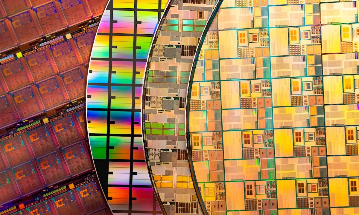

As semiconductor architectures move toward increasingly dense, fine-pitch interconnects, the reliance on high-performance materials to maintain mechanical and thermal integrity has become a primary bottleneck in electronics manufacturing. A collaborative research team from the National Institute of Standards and Technology (NIST), the University of California, San Diego (UCSD), and other industry partners has released a comprehensive study that establishes a new predictive framework for the behavior of highly filled epoxy underfills. By utilizing a combination of differential scanning calorimetry (DSC), thermogravimetric analysis (TGA), and diffusion-incorporated kinetic modeling, the study offers a rigorous methodology for quantifying the lifecycle of these materials, from initial oven curing to long-term thermal endurance.
The Role of Underfills in Modern Packaging
Advanced packaging technologies, such as flip-chip and 3D integrated circuits (ICs), involve stacking silicon dies with extremely high I/O counts. The interconnects between these layers are susceptible to significant thermomechanical stresses caused by the mismatched coefficients of thermal expansion (CTE) between the silicon chip and the organic substrate. Epoxy underfills act as the critical buffer, flowing into the gaps between the die and the substrate to encapsulate solder joints and redistribute these mechanical loads.
However, the efficacy of an underfill is intrinsically tied to its cure state. If an underfill is under-cured, it fails to provide the necessary mechanical support; if over-processed, it may degrade prematurely. The challenge for manufacturers lies in the "highly filled" nature of modern underfills, which incorporate ceramic or silica particles to tune CTE and modulus. These fillers complicate the chemical kinetics of the curing process, often leading to diffusion-controlled phenomena that are difficult to model using standard industrial protocols.
Chronology and Methodology of the NIST-Led Investigation
The research project, which culminated in the August 2026 publication in the Journal of Polymer Science, followed a multi-year effort to standardize the assessment of thermoset performance. The investigation proceeded through four distinct phases:
- Material Preparation and Cryomilling: To overcome the inherent inconsistencies in highly filled epoxy samples, the team employed cryomilling. By cooling the samples to cryogenic temperatures before pulverizing them, the researchers achieved a homogeneous powder without triggering premature chemical reactions or oxidative degradation. This ensured that subsequent thermal analysis would yield reproducible results.
- Kinetic Characterization: The team utilized isoconversional analysis to determine the apparent activation energy of the curing process. The data revealed that activation energy is not constant but varies significantly with the degree of conversion, showing a sharp increase as the epoxy approaches vitrification.
- Kinetic Modeling: To predict behavior in a real-world manufacturing environment, the team implemented a two-step modified Kamal–Sourour model. This model specifically accounts for diffusion-controlled reactions in the final stages of the cure, allowing for accurate prediction of conversion levels after the material transitions into a glass-like state.
- Thermal Endurance Testing: Using the ASTM E1641 and E1877 protocols, the researchers subjected the cured samples to thermogravimetric analysis to establish a 5% mass-loss criterion. This provided a definitive metric for the thermal lifespan of the material under nitrogen atmospheres.
Data Analysis: Understanding Diffusion-Controlled Curing
The study’s findings highlight a critical technical nuance: the transition from chemical-controlled to diffusion-controlled curing. In the early stages of the curing cycle, the reaction rate is determined by the collision frequency of reactive species. As the epoxy network builds, the mobility of these species decreases, causing the reaction rate to plummet.
The researchers discovered that conventional models often underestimate the time required to reach a "nearly complete cure." By integrating diffusion factors into the Kamal–Sourour model, the team successfully predicted the conversion profiles under varied oven schedules. This is particularly relevant for high-volume manufacturing, where oven residence time is a primary driver of cost and throughput. The ability to optimize this schedule—ensuring maximum cure without excessive thermal energy consumption—represents a significant efficiency gain for semiconductor assembly lines.
Implications for Semiconductor Reliability
The implications of this research extend to the fundamental reliability of consumer and industrial electronics. As electronic devices are subjected to more rigorous thermal cycling—such as in automotive under-the-hood applications or high-performance computing (HPC) data centers—the long-term stability of the underfill becomes the primary defense against solder joint fatigue.
The 5% mass-loss criterion established in the study serves as a predictive proxy for chemical degradation. By mapping this mass loss against temperature, the NIST and UCSD team provided a quantitative framework that allows material scientists to extrapolate the "service life" of an underfill. This data-driven approach moves the industry away from "trial-and-error" testing, which has historically been the standard for new material qualification. Instead, manufacturers can now use the team’s model to simulate the impact of different thermal environments on the underfill’s integrity before the hardware ever hits the production line.
Industry Reaction and Contextual Significance
While this paper focuses on the technical nuances of epoxy chemistry, the broader industry has recognized the need for such predictive frameworks. Semiconductor industry analysts note that the complexity of advanced packaging—including the shift toward hybrid bonding and larger interposers—has made "black box" materials performance unacceptable.
"The shift toward predictive modeling in polymer chemistry is a necessity for the next generation of semiconductor manufacturing," says an independent materials science consultant familiar with the study. "For years, the industry relied on empirical data that was often specific to a single oven configuration. By decoupling the kinetic behavior from the specific thermal equipment, this team has provided a universal toolkit that can be applied to any high-fill epoxy system."
Furthermore, the integration of ASTM standard protocols (E1641/E1877) into the research ensures that the results are not only academically rigorous but also commercially actionable. Manufacturers looking to implement these findings can follow the standardized procedures to validate their own proprietary underfill formulations, thereby reducing the time-to-market for new high-performance packaging solutions.
Challenges in Highly Filled Systems
The study also sheds light on the limitations of working with highly filled systems. The presence of inorganic fillers, while essential for thermomechanical stability, introduces "boundary effects" at the interface between the filler and the epoxy resin. These interfaces can act as nucleation sites or, conversely, as regions of lower cross-link density.
The researchers observed that the cryomilling process was instrumental in bypassing these complexities. By creating a uniform distribution of filler and resin, the team was able to treat the underfill as a cohesive system, allowing for the application of the modified Kamal–Sourour model. This suggests that future material development might focus on surface-treating these fillers to ensure they participate more actively in the curing network, rather than merely acting as inert structural components.
Future Outlook and Technological Integration
The framework developed by the NIST and UCSD team is expected to be integrated into computer-aided engineering (CAE) software packages used by packaging engineers. As digital twins become more prevalent in the design of semiconductor components, the ability to feed these kinetic parameters into a simulation allows designers to predict the structural health of an IC package throughout its projected multi-year lifespan.
Moreover, as the industry pushes toward higher integration densities, the thermal envelope for these devices is narrowing. The research provides a clear roadmap for how material scientists can evaluate the trade-offs between processing speed and thermal stability. If a specific application requires higher thermal endurance, the predictive model can determine the exact oven curing profile required to achieve that state, effectively allowing for "on-demand" material property engineering.
The August 2026 report serves as a foundational document for the next phase of materials science in electronics. By bridging the gap between molecular-level curing kinetics and macro-scale thermal endurance, the study provides a robust, reproducible, and scalable methodology. As the industry continues to tackle the challenges of Moore’s Law at the packaging level, such quantitative approaches will be essential to ensuring that the structural foundations of our digital world remain stable under increasingly demanding conditions.
The full technical paper, including the detailed kinetic equations and thermal analysis data, is available through the NIST technical repository, providing a resource for engineers and researchers currently navigating the complexities of advanced semiconductor interconnects.
