
The semiconductor industry in 2026 has reached a pivotal juncture where the traditional "shift left" philosophy—once a conceptual goal for moving verification earlier in the design cycle—has become a foundational requirement for survival in an era of hyper-complex, software-defined hardware. As chip architectures transition toward multi-die systems and AI-accelerated workloads, the boundaries of the design flow have expanded, dragging traditionally late-stage processes like software bring-up, thermal analysis, and power characterization into the earliest phases of architectural definition. This shift is no longer merely about meeting a deadline; it is about ensuring that the final silicon, often costing tens of millions of dollars to produce at advanced nodes, actually meets the performance and power requirements of the modern data center and edge environments.
The Paradigm Shift: From Functional Verification to System-Level Validation
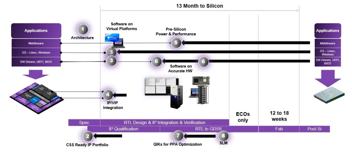
In the previous decade, "shift left" was primarily concerned with finding functional bugs in Register Transfer Level (RTL) code before tape-out. However, the industry landscape of 2026 presents a different set of challenges. Today, the leading cause of silicon re-spins is no longer just a failure of logic, but a failure of the system to perform under real-world workloads. The "hard boundary" of the design flow—the point at which the implementation is locked for manufacturing—now looms larger than ever. After this point, Engineering Change Orders (ECOs) become prohibitively expensive or physically impossible, particularly in 3D-IC (three-dimensional integrated circuit) structures where interconnects are fixed.
Industry data indicates that while functional verification remains a hurdle, nearly 40% of modern design failures are attributed to "parametric misses"—chips that function correctly in a vacuum but fail to hit power-per-watt targets or succumb to thermal throttling when running production-grade AI models. This has necessitated a move toward validating the entire software stack, including low-level drivers, operating systems, and middleware, long before a single transistor is etched.
A Chronology of Shift Left Maturity
The journey toward the current 2026 standard has been marked by three distinct eras of technological evolution:
- The Modular Era (2000s–2010s): Verification was siloed. Hardware teams focused on RTL, while software teams waited for "golden" models or early silicon samples. The shift left was limited to basic simulation and the early adoption of hardware emulation for the largest Tier-1 semiconductor firms.
- The Integration Era (2015–2022): The rise of mobile and early AI led to the adoption of FPGA-based prototyping. This allowed for tens of megahertz of performance, enabling software teams to begin work months earlier. However, power and thermal analysis remained "tail-end" activities.
- The Multiphysics and AI Era (2023–Present): In 2026, the flow is a continuous loop. Virtual prototypes are deployed during the specification phase, and AI agents now automate the transition between abstraction levels. Power and thermal data are now generated using activity vectors from real software running on emulators, allowing for "thermal-aware" architectural decisions.
The Tooling Continuum: Virtual Prototypes to FPGA Prototyping
To achieve this deep level of integration, the 2026 design toolkit has matured into a seamless continuum. At the furthest "left" of the schedule, designers utilize virtual prototypes. These are high-level software models of the hardware that can execute production code at high speeds. While they lack the cycle-accuracy of a final netlist, they allow architects to feed actual AI workload data into early power analysis tools. This is critical for high-speed interfaces such as PCI Express 6.0/7.0 and UCIe (Universal Chiplet Interconnect Express), where the protocol complexity requires early validation.
As the design firms up, the workload transitions to hardware emulation. Modern emulation systems now support multi-billion gate designs, providing the capacity to host entire "system-of-chips" environments. Companies like Rebellions have successfully utilized this phase to run AI accelerator logic alongside virtualized compute subsystems. By optimizing how data cycles move between the accelerator and the CPU before the hardware is finalized, they have significantly reduced the risk of performance bottlenecks.
The final stage of the pre-silicon continuum is FPGA-based prototyping. By running at speeds approaching 50-100 MHz, these systems allow for full-scale software compliance and certification work. This is where organizations like AMI validate BIOS and firmware against integrated subsystems, ensuring that the "first-silicon" experience is a bootable experience, not a debugging marathon.
Beyond Function: The Rise of Pre-Silicon Multiphysics
Perhaps the most significant advancement in 2026 is the integration of multiphysics into the shift-left workflow. For years, power analysis was based on "worst-case" estimates or static spreadsheets. Today, the activity data generated by emulators—representing actual software execution—is fed directly into computationally intensive thermal and structural models.

This allows engineers to visualize hotspots on the die and identify potential IR drop (voltage sag) issues that only occur during specific software routines. By knowing the genuine maximum thermal envelope for actual workloads, teams can design more aggressive cooling solutions or choose more cost-effective packaging. Furthermore, this analysis now extends to structural integrity, predicting die warpage and mechanical stress in multi-die packages before the expensive assembly process begins.
The Role of Agentic AI and Spec Engineering
As design complexity scales, human engineers are increasingly supported by "agentic AI." These are autonomous AI agents capable of running and optimizing the verification process itself. In 2026, these agents are used to:
- Automate Workload Porting: Moving complex software stacks onto virtual prototypes and emulators with minimal manual configuration.
- Spec-to-Implementation Mapping: Using AI to ensure that the design specification is accurately reflected in the hardware implementation, reducing the "intent-to-execution" gap.
- Predictive Debugging: Identifying the root cause of failures in massive simulation logs before a human engineer even opens the file.
This "spec engineering" ensures that more of a design’s destiny is decided in the digital realm, where mistakes are reversible, rather than in the fab, where they are catastrophic.
Industry Implications: Aerospace, Defense, and Mission-Critical Systems
The implications of these advanced shift-left methodologies extend beyond consumer electronics. In the aerospace and defense sectors, the connection between Model-Based Systems Engineering (MBSE) and chip design has become a primary focus. At the 2026 Design Automation Conference (DAC) in Long Beach, the integration of SysML (Systems Modeling Language) with semiconductor design flows is expected to be a central theme.
For mission-critical applications, the ability to define requirements independently of hardware/software decisions allows for a "chips-to-missions" approach. Engineers can simulate how a specific processor will perform within a larger satellite or avionics system, ensuring that the hardware meets the mission requirements before the first chip is ever manufactured. This level of system-level modeling, which once seemed like "wishful thinking," is now a standard part of the high-reliability design flow.
Economic Impact and Future Outlook
The economic reality of 2026 is that the cost of a 2nm or 3nm design cycle can exceed $500 million when accounting for IP licensing, EDA tools, and engineering talent. In this high-stakes environment, the ability to shift left is the difference between market leadership and financial failure. By leveraging pre-integrated subsystems—such as Arm compute clusters paired with Synopsys IP—developers can focus their "differentiation budget" on unique features rather than reinventing standard interfaces like DDR or USB.
The data supports this trend: companies that successfully implement a full-stack shift-left strategy report a 25-30% reduction in overall time-to-market and a significantly higher rate of "right-first-time" silicon that meets all power and performance targets.
As the line on the whiteboard continues to extend further to the left, the role of the engineer is evolving. The challenge is no longer just managing gates and transistors, but managing the immense complexity of multiphysics, software stacks, and AI-driven optimization. In 2026, the "great shift to the left" has reached its logical conclusion: the design of a chip is now inseparable from the design of the system it inhabits. The tools and methodologies have finally caught up to the ambitions of the architects, enabling a new era of silicon innovation that is as much about software and physics as it is about logic.
