
The semiconductor industry is currently undergoing a foundational shift in how integrated circuits are designed, manufactured, and assembled, moving away from the traditional monolithic System-on-Chip (SoC) model toward a more modular, "chiplet-based" architecture. At the heart of this transition is the Universal Chiplet Interconnect Express (UCIe), an open industry standard that has matured rapidly since its introduction in March 2022. What began as a foundational protocol for basic die-to-die connectivity has evolved into a sophisticated ecosystem capable of managing secure data movement, complex power delivery, and rigorous validation across diverse packaging technologies. This evolution is critical as the industry faces the physical and economic limits of Moore’s Law, necessitating a new way to scale performance without relying solely on transistor shrinkage.
The Genesis and Strategic Necessity of UCIe
The formation of the UCIe Consortium was a watershed moment for the semiconductor world, bringing together traditional rivals such as Intel, AMD, Arm, and Nvidia, alongside leading foundries like TSMC and Samsung, and cloud giants like Google and Microsoft. The primary driver for this collaboration was the "reticle limit" problem. As high-performance computing (HPC) and artificial intelligence (AI) applications demand more processing power, die sizes have expanded to the point where they occupy nearly the entire area of a lithography reticle (approximately 858mm²). Manufacturing such large monolithic dies is prohibitively expensive due to lower yields; a single defect can ruin the entire chip.
By breaking a large design into smaller "chiplets," manufacturers can improve yields significantly. Smaller dies have a higher probability of being defect-free, and different functions can be manufactured on the most appropriate process nodes—for instance, using a 3nm process for the CPU cores while keeping the I/O and analog components on more cost-effective 7nm or 12nm nodes. However, for this modular approach to work, these separate pieces of silicon must communicate with the same speed, latency, and reliability as if they were on the same die. UCIe was established to provide this standardized "glue."
Chronology of Development: From 1.0 to 1.1 and Beyond
The timeline of UCIe reflects the urgent pace of innovation in the data center and AI sectors. In March 2022, UCIe 1.0 was released, focusing on the fundamental physical layer and link layer specifications. It established the groundwork for two types of packaging: standard (organic substrate) and advanced (silicon interposer, fan-out, or bridge-based). This initial release provided a high-bandwidth, low-latency interface that leveraged existing software ecosystems by supporting PCIe and CXL protocols.
By August 2023, the consortium released UCIe 1.1, which introduced critical enhancements for broader industry adoption. This update focused on three key areas: automotive-grade reliability, enhanced testing and compliance, and expanded streaming protocols. The inclusion of automotive specifications was particularly significant, as the transition to software-defined vehicles requires massive localized computing power, often necessitating chiplet-based designs for redundancy and scalability. Furthermore, the 1.1 update introduced "Raw Mode," allowing for even lower latency by bypassing certain protocol overheads for specialized applications.
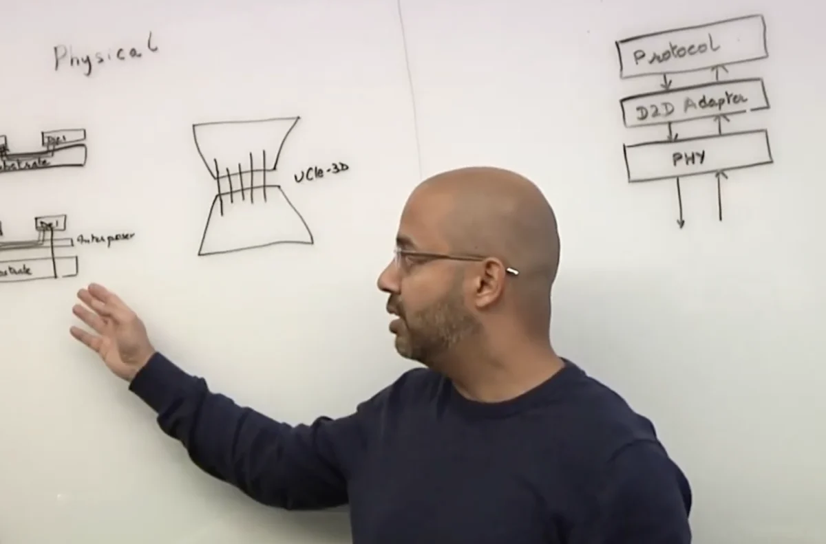
Technical Architecture: Layers of Connectivity
To understand the maturation of the standard, one must examine the multi-layered approach UCIe takes toward data movement. Mayank Bhatnagar, director of product marketing at Cadence, notes that the standard is designed to be flexible enough to handle everything from simple point-to-point connections to complex multi-foundry integrations.

The Physical Layer
At the base of the stack is the physical layer (PHY), which defines the electrical signaling, the "bumps" (the microscopic solder balls that connect the chip to the package), and the channel characteristics. UCIe supports a wide range of data rates, typically starting at 4 Gbps per lane and scaling up to 32 Gbps and beyond. In advanced packaging, these lanes are packed extremely tightly, providing a massive aggregate bandwidth.
The Die-to-Die (D2D) Adapter
Above the PHY is the D2D adapter, which manages link state, flow control, and error detection. One of the most significant evolutions in the UCIe standard is how this layer handles "Sideband" signaling. Sideband is a dedicated, low-speed communication channel that allows chiplets to "talk" to each other about their status, power requirements, and thermal limits before the high-speed data transmission even begins. This is essential for ensuring that a chiplet from Foundry A can safely initialize and synchronize with a chiplet from Foundry B.
The Protocol Layer
The top layer allows for the seamless integration of industry-standard protocols. By supporting PCIe (Peripheral Component Interconnect Express) and CXL (Compute Express Link), UCIe ensures that software developers do not need to rewrite their code to support chiplet-based hardware. To the operating system, a collection of chiplets connected via UCIe appears as a single, high-performance logical entity.
Supporting Data: Performance and Efficiency Metrics
The shift toward UCIe is driven by measurable gains in power efficiency and bandwidth density. Traditional off-chip communication (like standard PCIe between two separate chips on a PCB) consumes a significant amount of energy—often measured in tens of picojoules per bit (pJ/bit). In contrast, UCIe aims for an order of magnitude improvement.
Data from the UCIe Consortium indicates that for advanced packaging, the standard can achieve power efficiency as low as 0.5 pJ/bit. This is critical for AI training clusters, where energy costs and heat dissipation are the primary bottlenecks. In terms of bandwidth density, UCIe can provide up to 1,350 Gbps per millimeter of die edge (linear density) and even higher area density in 3D configurations. This allows designers to move terabits of data per second between a processor and its high-bandwidth memory (HBM) with minimal physical footprint.
Industry Perspectives and the Multi-Foundry Challenge
A major hurdle for the chiplet ecosystem is interoperability. Historically, die-to-die interfaces were proprietary (e.g., AMD’s Infinity Fabric or Intel’s EMIB). The success of UCIe depends on the ability of a "chiplet marketplace" to emerge, where a designer could theoretically buy a specialized AI accelerator chiplet from one vendor and pair it with a general-purpose CPU chiplet from another.
Cadence and other Electronic Design Automation (EDA) providers have been vocal about the need for standardized verification and testing. Mayank Bhatnagar highlights that as the standard has matured, the focus has shifted from "can we connect these?" to "how do we validate them at scale?" This includes "Known Good Die" (KGD) testing—the process of ensuring each chiplet is fully functional before it is permanently bonded into an expensive multi-chip package. If one chiplet in a ten-chiplet package is faulty, the entire assembly may be lost, making robust testing protocols a financial necessity.

Foundries have also reacted by aligning their packaging roadmaps with UCIe. TSMC’s CoWoS (Chip on Wafer on Substrate) and Intel’s Foveros technologies are increasingly optimized to support UCIe-compliant interfaces, providing a physical infrastructure that matches the logical requirements of the standard.
Broader Implications: AI, Automotive, and the Future of Computing
The implications of UCIe’s maturation extend far beyond the server room. In the realm of Artificial Intelligence, the ability to mix and match memory and logic chiplets allows for more granular optimization of "AI at the Edge." For example, a surveillance camera might use a low-power image processing chiplet paired with a specialized neural engine, all housed in a single, compact package.
In the automotive sector, UCIe provides a path toward the "Central Compute" architecture. Modern vehicles are moving away from having dozens of small Electronic Control Units (ECUs) toward a single, powerful central brain. UCIe allows automotive manufacturers to scale this central processor by adding chiplets as vehicle features (like autonomous driving levels) increase, without redesigning the entire system-on-chip from scratch.
Furthermore, the standard is a prerequisite for the eventual rise of 3D-IC (3D Integrated Circuits), where chiplets are stacked vertically rather than side-by-side. Vertical stacking further reduces the distance data must travel, potentially pushing power efficiency well below the 0.5 pJ/bit mark and enabling a new generation of "brain-scale" computing devices.
Conclusion
The Universal Chiplet Interconnect Express has transitioned from a promising proposal into a robust, indispensable pillar of modern semiconductor engineering. By standardizing the physical and logical layers of die-to-die communication, it has unlocked the potential of heterogenous integration, allowing the industry to continue its march toward higher performance in the face of daunting physical constraints. As the ecosystem continues to grow, the focus will likely shift toward further security enhancements and the refinement of a global chiplet supply chain, ensuring that the modular future of silicon is as secure and reliable as the monolithic past. Through the collaborative efforts of EDA vendors, foundries, and chip designers, UCIe is not just connecting dies; it is connecting the future of the digital world.
