
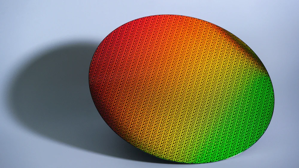
Intel Foundry has unveiled a series of significant advancements in semiconductor manufacturing at the 2026 IEEE/JSAP Symposium on VLSI Technology & Circuits, marking a pivotal moment in the company’s "five nodes in four years" roadmap. The presentation, centered on the transition to the "Angstrom Era," highlighted the introduction of Intel 18A-P, the first performance-enhanced version of the Intel 18A node. Now in the risk production phase, Intel 18A-P represents a critical evolution in gate-all-around (GAA) transistor architecture and backside power delivery, technologies that Intel views as essential for the high-performance demands of the artificial intelligence (AI) economy. Through a series of six technical papers, Intel engineers demonstrated how these innovations resolve long-standing structural bottlenecks in chip design, offering substantial gains in frequency, power efficiency, and area scaling.
The Evolution of Intel 18A-P and the Power Boost Architecture
The flagship announcement at the symposium was the Intel 18A-P process, which builds upon the foundational Intel 18A node while maintaining design-rule compatibility. This compatibility is a strategic move by Intel Foundry, allowing customers to migrate existing layouts and libraries to the enhanced node without the prohibitive costs of a total redesign. The "P" designation signifies a performance boost driven by refined device options, tighter variation control, and improved interconnect metallization.
A standout feature of this new node is "Power Boost," the industry’s first implementation of a dual-contact architecture enabled by PowerVia backside power delivery. Traditionally, transistors rely on frontside contacts that compete for space with signal routing. Power Boost utilizes both frontside and direct backside contacts to the PowerVia, significantly reducing electrical resistance for both NMOS and PMOS transistors. According to silicon-validated data presented by Intel, fully routed blocks using an industry-standard ARM core sub-block demonstrated a 9% performance gain at 0.75V compared to the standard Intel 18A. Conversely, at the same performance level, the 18A-P node achieved an 18% reduction in power consumption.
Furthermore, Intel 18A-P addresses the thermal challenges inherent in high-density AI accelerators and data center processors. By implementing material innovations and enhancing electronic design automation (EDA) workflows, Intel has achieved a 20% to 40% improvement in the thermal resistance of the overall chip stack. This thermal headroom is vital for maintaining high clock speeds in sustained workloads without triggering aggressive thermal throttling.
Structural Transformation: GAA Transistors and Backside Power
For decades, the semiconductor industry relied on FinFET (Fin Field-Effect Transistor) architecture. However, as transistors shrunk toward the 2nm and 1.8nm levels, FinFETs began to face limitations in power delivery and electrostatic control. Intel’s transition to RibbonFET (its proprietary GAA implementation) and PowerVia (backside power delivery) is designed to overcome these hurdles.
Research presented at the VLSI Symposium highlighted a critical discovery: the synergy between GAA and backside power allows for much more efficient operation at low voltages. In tests involving CPU cores, GAA designs with backside power achieved core frequencies approximately 30% higher than FinFET-based designs at an operating voltage of 0.5V. This breakthrough is particularly relevant for the "AI Edge" and mobile sectors, where devices must balance high computational bursts with strict battery life constraints. By enabling stable operation at 0.5V—a threshold previously considered impractical for high-performance compute—Intel is opening the door for a new generation of energy-efficient mobile SoCs.
The move to the backside of the wafer for power delivery also solves the "congestion crisis" on the frontside of the chip. In traditional designs, power and signal wires are interleaved on the same metal layers, leading to interference and routing bottlenecks. By shifting the power delivery network (PDN) to the rear, Intel freed up the frontside for signal routing, resulting in an 11% reduction in total cell area. This allows for shorter wire lengths and fewer vias, which in turn reduces the parasitic capacitance that often degrades signal integrity.

Mitigating Voltage Droop and Enhancing Reliability
One of the most technical yet impactful data points shared at the symposium concerned "dynamic voltage droop." As processors switch between idle and high-load states, sudden demands for current can cause a momentary drop in voltage (IR drop). If this droop is too severe, the circuit fails. To prevent this, designers typically add "guardbands," which essentially slow down the chip to ensure stability.
Intel’s data showed that the Intel 18A platform, utilizing backside power, reduced peak dynamic voltage droop to under 10 mV. In comparison, the Intel 3 node, which uses conventional frontside power, exhibited droops of more than 90 mV. This 10-fold reduction in voltage instability allows engineers to tighten guardbands, resulting in a 5% to 6% frequency uplift or up to a 15% reduction in total power consumption. This stability is a cornerstone of Intel Foundry’s pitch to designers of high-performance computing (HPC) and AI training hardware, where consistent voltage is paramount for massive parallel processing.
Breakthroughs in GaN and CFET Research
Beyond the immediate 18A roadmap, Intel Foundry shared long-term research into Gallium Nitride (GaN) and Complementary FET (CFET) technologies. GaN has long been prized for its efficiency in power electronics, but integrating it onto high-volume 300mm silicon logic wafers has been a historic challenge.
In collaboration with the University of California, San Diego, Intel demonstrated the integration of efficient digital logic on a 300mm GaN-on-Silicon platform. The team used a hybrid approach, combining GaN nMOS with silicon pMOS to create digital control circuits. This research achieved a power-delay product (PDP) of 6.2 attojoules per stage—a staggering 1,000-fold improvement in efficiency over previous GaN logic attempts. This suggests a future where power management and logic can be integrated on a single die, drastically reducing the size and cost of power delivery systems in everything from smartphones to electric vehicles.

Intel also provided an update on CFET (Complementary FET) integration. CFET represents the next step after GAA, where NMOS and PMOS transistors are stacked vertically on top of one another. Intel successfully demonstrated a CFET logic circuit at a 45nm gate pitch, utilizing a 2×2 ribbon stack. This research included the use of "epi-epi vias" for vertical connections and a selective "device depopulation" technique to reduce manufacturing complexity. CFET technology promises to nearly double the transistor density of current GAA nodes, providing a path for continued Moore’s Law scaling into the 2030s.
Material Innovation: Ruthenium Interconnects and Airgaps
As interconnect pitches become tighter, the resistance of traditional copper wiring increases exponentially. To combat this, Intel presented research on subtractive Ruthenium (sRu) interconnects combined with airgap insulation. This marks the first time such a metallization scheme has been integrated with functional RibbonFET devices on a test chip.
The results indicated that at matched leakage levels, the Ruthenium and airgap scheme improved circuit performance by approximately 2%. More importantly, the use of airgaps reduced capacitance by up to 35% compared to conventional dielectric materials. Furthermore, the research showed a 50% reduction in via resistance, ensuring that vertical connections between metal layers remain fast and efficient. These material science breakthroughs are essential for maintaining the speed of data transfer within the chip as the physical dimensions of the wires continue to shrink.
Strategic Chronology and Industry Implications
The announcements at VLSI 2026 represent the culmination of a multi-year strategic pivot initiated by Intel CEO Pat Gelsinger in 2021. The timeline began with the rebranding of nodes (Intel 7, Intel 4, Intel 3) and moved toward the introduction of the Angstrom era with Intel 20A and 18A.

- 2021-2023: Intel focused on regaining process leadership through the refinement of FinFET on Intel 7 and the introduction of EUV (Extreme Ultraviolet) lithography on Intel 4 and Intel 3.
- 2024-2025: The transition to GAA (RibbonFET) and Backside Power (PowerVia) began with the internal ramp of Intel 20A.
- 2026: Intel 18A enters high-volume manufacturing, while 18A-P moves into risk production, signaling the readiness of the foundry for external customers like Microsoft, Amazon, and potentially NVIDIA.
The broader implications of these developments are profound. By successfully executing on backside power delivery ahead of its primary competitors, TSMC and Samsung, Intel Foundry is positioning itself as the preferred destination for AI chip startups and established giants alike. The 11% area reduction and 30% frequency gains at low voltage provide a tangible "PPA" (Power, Performance, and Area) advantage that is critical in the competitive landscape of AI accelerators.
Conclusion: From Theory to Execution
The data presented at the 2026 IEEE/JSAP Symposium on VLSI Technology & Circuits suggests that Intel Foundry has moved beyond the theoretical stages of its turnaround. The transition from lab research to silicon-validated benchmarks for Intel 18A-P demonstrates a mature execution of the GAA and PowerVia architectures.
As the industry looks toward the next decade of compute, Intel’s investment in GaN, CFET, and Ruthenium interconnects provides a clear roadmap for sustaining performance gains. For customers, the message is one of stability and innovation: Intel Foundry is not only catching up to the leading edge but is actively defining the manufacturing standards for the AI era. The combination of Power Boost, improved thermal management, and 300mm GaN integration suggests that the next generation of silicon will be defined by structural efficiency as much as by raw transistor counts.
