
The global semiconductor industry is currently navigating a pivotal transition as traditional scaling methods approach their physical limits, prompting a surge in radical architectural redesigns. Recent breakthroughs from the Okinawa Institute of Science and Technology (OIST), the Korea Advanced Institute of Science and Technology (KAIST), and a collaborative team from Zhejiang and RMIT Universities are poised to redefine the three most critical pillars of modern microelectronics: lithographic precision, thermal management, and integrated optical sensing. These advancements address the escalating costs of sub-3nm manufacturing, the "thermal wall" hindering artificial intelligence (AI) processors, and the need for miniaturized spectral analysis in consumer electronics.
Redesigning High-NA EUV: A New Economic Paradigm for Sub-3nm Manufacturing
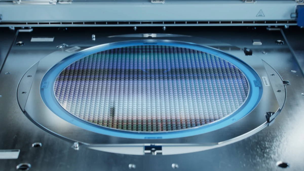
As the semiconductor roadmap moves toward the 2nm node and beyond, the industry has become increasingly reliant on High-Numerical Aperture (High-NA) Extreme Ultraviolet (EUV) lithography. However, the current implementation of this technology, pioneered primarily by ASML, involves machines that cost upwards of €350 million per unit, creating a massive financial barrier for all but the largest foundries. Tsumoru Shintake, a professor at the Okinawa Institute of Science and Technology (OIST), has proposed a radical redesign of the illumination and projection systems that could potentially reduce these costs by 75%.
The OIST proposal focuses on the fundamental optical path within the lithography machine. In traditional EUV systems, the complex arrangement of mirrors required to maintain a high numerical aperture often leads to significant light loss and optical aberrations. Every reflection in an EUV system results in a loss of approximately 30% of the light intensity, meaning that a system with 10 to 12 mirrors delivers only a fraction of the source power to the wafer.
Professor Shintake’s design utilizes a simplified collector mirror system in the illumination unit to bring short-wavelength EUV light to the photomask with higher efficiency. The core innovation lies in the "in-line" projector design, where multiple reflections are carefully arranged to cancel out optical defects. This geometric symmetry allows the system to maintain a high numerical aperture while using fewer, more easily manufactured mirrors. According to Shintake, this design can achieve 2-3 nm scale details while being significantly simpler to produce than current state-of-the-art machines.
The economic implications are profound. If a High-NA EUV machine can be produced at a quarter of the current market cost, the democratization of advanced node manufacturing could shift the competitive landscape. "This design can make high-NA technology much simpler and cheaper to produce, opening new possibilities for semiconductor manufacturing," Shintake stated. The OIST research suggests that by reducing the complexity of the optical train, foundries could see a lower Total Cost of Ownership (TCO) and higher throughput due to reduced light attenuation.
Embedded Liquid Cooling: Piercing the 2,000-Watt Thermal Barrier
While OIST addresses the fabrication of chips, researchers at the Korea Advanced Institute of Science and Technology (KAIST) are solving the problem of operating them. The rise of AI and high-performance computing (HPC) has led to power densities that exceed the capabilities of conventional air and even standard liquid cooling. Modern AI accelerators, such as those used in large-scale data centers, generate intense localized heat that can cause thermal throttling or hardware failure.
The KAIST team, led by Professor Sung Jin Kim of the Department of Mechanical Engineering, has developed a Manifold MicroChannel (MMC) structure embedded directly into the silicon chip. Unlike traditional "cold plates" that sit on top of the chip packaging, the MMC system integrates cooling channels into the silicon itself, bringing the coolant—room-temperature water—within microns of the heat-generating transistors.
In testing, this embedded system maintained chip temperatures below 100°C even under extreme heat generation conditions exceeding 2,000 watts per square centimeter (W/cm²). To put this in perspective, the heat flux of a typical high-end CPU is roughly 100-300 W/cm², while the surface of the sun is approximately 6,000 W/cm². The KAIST design manages this load through a sophisticated distribution network that uses multiple inlets and outlets. This "manifold" approach shortens the distance the coolant must travel across the chip, which drastically reduces flow resistance and the pumping pressure required to move the fluid.
The performance metrics of the KAIST system are unprecedented. The researchers reported a coefficient of performance (COP) of 106,000. This means the system can remove a massive amount of heat using only about one-tenth of the pumping power required by previous microchannel designs. Furthermore, the fabrication process remains compatible with existing semiconductor manufacturing, as it uses a low-temperature process (below 350°C). This compatibility is crucial for mass adoption, as it allows cooling channels to be integrated during the backend-of-line (BEOL) processing without damaging sensitive transistor structures.

Light Wavelength Analysis: Integrating Spectrometers into Standard Sensors
The third pillar of this technological shift involves the integration of complex sensing capabilities directly into imaging hardware. Researchers from Zhejiang University and RMIT University have demonstrated a method to build light wavelength analysis (spectrometry) directly into a standard camera chip. Traditionally, spectrometers are bulky instruments that require separate optical paths, diffraction gratings, and sensors, making them difficult to integrate into smartphones or wearable devices.
The team utilized ultrafast laser pulses to create microscopic spiral-shaped structures, or "micro-vortices," inside transparent materials. These structures are placed in front of a specialized optical system that can be integrated with a commercial image sensor. When incoming light hits these spiral structures, it is broken into distinct, wavelength-dependent patterns. These patterns are not "images" in the traditional sense but are instead data-rich spatial distributions that a sensor can interpret.
Professor Baohua Jia of RMIT’s Centre for Atomaterials and Nanomanufacturing (CAN) emphasized that this is a physical breakthrough rather than a software one. "It introduces a new physical component that separates light at a very small scale, close to the sensor itself," Jia explained. By using these micro-vortices, the chip can perform hyperspectral imaging—detecting the specific chemical signatures of objects by analyzing how they reflect or emit different wavelengths of light.
The team successfully integrated these structures with commercial CMOS sensors, proving that microscopic spectral imaging is feasible without the need for large external components. Bo Zhang of Zhejiang University noted that the next phase of the research will focus on scaling up fabrication and refining the reconstruction algorithms used to turn the light patterns into actionable spectral data. This technology could lead to smartphones capable of analyzing food safety, detecting skin conditions, or monitoring environmental pollutants in real-time.
Chronology of Development and Industry Context
The timeline of these breakthroughs suggests a synchronized push toward a new generation of hardware by the late 2020s.
- June 2026: Professor Tsumoru Shintake publishes the "High-NA in-line projector" design in the Journal of Micro/Nanopatterning, Materials, and Metrology, providing a theoretical and experimental framework for a cheaper EUV alternative.
- Mid-2026: The KAIST team publishes their findings on MMC cooling in Energy Conversion and Management, demonstrating the 2,000 W/cm² threshold.
- 2026: The Zhejiang and RMIT collaboration publishes in Nature Electronics, showcasing the first integrated micro-vortex spectrometer on a commercial sensor.
This cluster of innovations arrives at a time when the semiconductor industry is facing "the end of Moore’s Law" in its traditional sense. As transistors can no longer be shrunk without massive increases in power and cost, the industry is looking toward "More than Moore" strategies—enhancing the functionality and efficiency of the chip rather than just its density.
Analysis of Broader Impacts and Market Implications
The convergence of these three technologies could reshape several multi-billion dollar industries. In the lithography sector, the OIST design poses a theoretical challenge to the current monopoly on High-NA EUV equipment. While ASML’s systems are already being deployed at Intel and TSMC, the high cost of these machines risks pricing out smaller players and secondary markets. A "quarter-cost" alternative could allow for a more diverse manufacturing ecosystem, potentially bringing advanced node capabilities to regions currently lagging in the semiconductor race.
In the data center and AI sector, the KAIST cooling solution addresses the single greatest operational cost: electricity and thermal management. Data centers currently consume roughly 1-2% of global electricity, with a significant portion of that power going toward cooling fans and chillers. By using embedded liquid cooling with a COP of over 100,000, operators could drastically reduce their energy footprint while pushing their AI chips to higher clock speeds without the risk of thermal failure.
Finally, the Zhejiang/RMIT optical sensor breakthrough moves the industry closer to the "Internet of Everything" (IoE). By turning every smartphone camera into a laboratory-grade spectrometer, the technology enables a new class of consumer-facing health and safety applications. This shift from "image capture" to "material analysis" represents a fundamental change in how we interact with the physical world through our devices.
Conclusion
The research presented by OIST, KAIST, and the Zhejiang/RMIT partnership represents a holistic advancement in semiconductor technology. By addressing the cost of fabrication, the limits of thermal physics, and the integration of advanced sensing, these researchers are providing the tools necessary for the next decade of digital transformation. As these technologies move from the laboratory to the fabrication plant, the industry may find that the most significant leaps in performance come not from shrinking the transistor further, but from reimagining the systems that build, cool, and empower them.
