

The global semiconductor landscape reached a significant milestone on June 18, 2026, as ASE (Advanced Semiconductor Engineering) officially unveiled its latest advancements in panel-level packaging (PLP) technology. This strategic shift aims to address the increasingly complex requirements of the artificial intelligence (AI) and high-performance computing (HPC) sectors, which have begun to outpace the physical and economic limitations of traditional wafer-level packaging (WLP). By transitioning to a larger rectangular format, ASE is positioning itself to provide the industry with a scalable solution that supports higher throughput, reduced cycle times, and a significantly lower cost per package. This evolution is particularly critical as the industry grapples with the diminishing efficiency of 300mm wafers when applied to the massive interposers required for next-generation multi-die architectures.
The Shift to Panel-Level Packaging: Addressing Industrial Bottlenecks
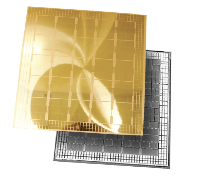
For decades, the semiconductor industry has relied on circular 300mm silicon wafers as the standard substrate for both chip fabrication and advanced packaging. However, the rise of "Extreme-size" packages—driven by the demand for AI accelerators and massive data center processors—has highlighted the inherent geometric inefficiencies of circular wafers. When a package size increases to accommodate multiple high-bandwidth memory (HBM) stacks and large logic dies, the number of packages that can fit on a single 300mm wafer drops precipitously. Furthermore, the "edge loss" on a circular wafer becomes more pronounced with larger rectangular dies, leading to wasted material and higher unit costs.
ASE’s panel-level platform utilizes a rectangular substrate that offers a significantly larger surface area than traditional wafers. While a standard 300mm wafer provides approximately 70,685 square millimeters of processing area, a typical 600mm x 600mm panel provides 360,000 square millimeters—a fivefold increase in usable space. This transition allows for the simultaneous processing of a much higher volume of units, effectively decoupling the manufacturing throughput from the physical constraints of the circular wafer format.
Technical Evolution and Chronology of ASE’s Packaging Roadmap
The move toward panel-level packaging is not an overnight development but the result of a decade-long roadmap focused on heterogeneous integration. To understand the significance of the 2026 announcement, it is essential to look at the chronology of advanced packaging milestones that led to this transition:
- 2016–2018: The Rise of Fan-Out Wafer-Level Packaging (FOWLP). ASE and other major OSATs (Outsourced Semiconductor Assembly and Test) perfected FOWLP to allow for higher I/O density without requiring a traditional substrate. This was primarily used for mobile applications.
- 2019–2022: The 2.5D and 3D Integration Era. As Moore’s Law began to slow, the industry turned to Chip-on-Wafer-on-Substrate (CoWoS) and other 2.5D technologies. ASE introduced its VIPack™ platform to facilitate the integration of logic and HBM.
- 2023–2024: The AI Infrastructure Explosion. The sudden demand for generative AI chips created a massive bottleneck in packaging capacity. Foundries and OSATs realized that the 300mm wafer format was becoming a limiting factor for the massive interposers (often 2x to 3x reticle size) used in AI GPUs.
- 2025: Pilot Programs for Panel-Level Fan-Out (PLFO). ASE began intensive testing of 310mm x 310mm and 600mm x 600mm glass and organic panels, focusing on overcoming the challenges of warpage and fine-pitch redistribution layer (RDL) lithography.
- June 2026: Commercial Readiness. ASE announces the full-scale deployment of its panel-level platform, specifically optimized for AI data centers, HPC, and high-end networking.
Supporting Data: Throughput and Cost Efficiency
The primary driver behind the adoption of PLP is the "cost-per-area" advantage. Internal data and industry projections suggest that the transition to panel-level processing can yield a 20% to 30% reduction in total packaging costs for large-die applications.
One of the most critical metrics in advanced packaging is "Area Utilization Efficiency." On a 300mm wafer, large AI packages often achieve only 60% to 70% area utilization due to the mismatch between the rectangular dies and the circular edge. In contrast, ASE’s panel-level format can achieve over 90% utilization.
Furthermore, the reduction in cycle time is a result of "Large-Area Processing" (LAP). In the RDL phase—where metal interconnects are formed to link different chips—a single exposure on a panel-level lithography tool can cover an area several times larger than a standard wafer stepper. This reduces the number of "shots" or steps required to process the same number of chips, directly translating to faster time-to-market for chip designers.
Addressing Complexity in Multi-Die Architectures
As AI models grow in parameters, the hardware required to run them becomes more complex. Modern AI accelerators often utilize a "chiplet" approach, where a central GPU or NPU is surrounded by six to eight HBM3e or HBM4 stacks. Integrating these components requires a massive interposer, which serves as the communication highway between the dies.
ASE’s panel-level platform is specifically engineered to handle these multi-die architectures. The platform supports:
- Heterogeneous Integration: Combining chips from different process nodes (e.g., a 3nm logic die with a 7nm I/O die) onto a single panel.
- Fine-Pitch RDL: Achieving line spacing and width that allow for the high-speed data transfer required by HPC applications.
- System-in-Package (SiP) Versatility: Enabling the integration of passive components, such as capacitors and inductors, directly into the package structure to improve power delivery and signal integrity.
Official Responses and Industry Stakeholder Perspectives
While ASE has led the charge, the transition to PLP is viewed by the broader industry as a necessary evolution. Analysts from leading semiconductor research firms have noted that the move is essential to prevent a "packaging plateau" where the cost of assembly outweighs the performance gains of the silicon.
"The industry has reached a point where the package is no longer just a protective shell; it is a fundamental component of the system’s performance," noted a senior analyst at a major technology research group following the announcement. "ASE’s commitment to panel-level formats provides a clear path for companies like Nvidia, AMD, and Intel to continue scaling their AI offerings without being hamstrung by the supply constraints of traditional wafer-based lines."
Foundry partners have also expressed support, as the offloading of advanced packaging to OSATs like ASE allows foundries to focus their high-end cleanroom capacity on front-end wafer fabrication. By standardizing panel-level processes, ASE is fostering an ecosystem where chip designers can design for a "rectangular world," optimizing their chiplet layouts for maximum panel yield.
Broader Impact and Market Implications
The implications of ASE’s panel-level platform extend far beyond the immediate cost savings. For the AI data center market, this technology is a prerequisite for the next generation of "Superchips." As data centers move toward liquid cooling and higher power densities, the ability to package larger, more integrated systems becomes a competitive advantage.
In the networking sector, the transition to 800G and 1.6T speeds requires optical engines and switch silicon to be co-packaged (Co-Packaged Optics or CPO). The panel-level format provides the necessary real estate to integrate these disparate technologies—silicon photonics, CMOS, and memory—into a single, high-efficiency footprint.
Furthermore, the "Edge AI" and high-end gaming markets stand to benefit. As edge devices require more local processing power to handle AI tasks without cloud latency, the cost-efficient SiP solutions enabled by PLP will allow for more powerful processors in smaller form factors, such as AR/VR headsets and autonomous vehicle compute modules.
Future Outlook: The Road to 2030
Looking ahead, ASE’s move into panel-level packaging is expected to trigger a wave of re-tooling across the OSAT industry. As the 2026 rollout matures, the focus will likely shift toward even larger formats and the integration of glass substrates. Glass offers superior flatness and thermal stability compared to organic materials, which will be necessary as die sizes continue to expand and interconnect densities reach sub-micron levels.
The announcement by ASE marks the end of the "wafer-only" era for high-end assembly. By embracing the panel format, the company is not only solving the throughput challenges of today but is also building the infrastructure required for the trillion-parameter AI models of tomorrow. As the semiconductor industry continues its shift toward "system-level" innovation, panel-level packaging will serve as the foundation upon which the next decade of computing is built.
In conclusion, ASE’s panel-level platform represents a fundamental shift in semiconductor manufacturing philosophy. By prioritizing area efficiency, throughput, and multi-die flexibility, ASE is providing the high-tech sector with the tools necessary to sustain the current pace of AI and HPC development. The transition reflects a maturing industry that is increasingly looking toward creative engineering and materials science to overcome the physical limits of traditional silicon processing.
