
The semiconductor landscape is undergoing a fundamental shift as the industry moves beyond traditional transistor scaling toward advanced packaging and heterogeneous integration. This evolution was on full display at the Electronic Components and Technology Conference (ECTC) held this week in Orlando, Florida. Industry leaders, researchers, and equipment manufacturers gathered to showcase innovations in panel-level packaging, hybrid bonding, and novel substrate materials, marking a pivotal moment in the quest to sustain performance gains in the post-Moore’s Law era. As artificial intelligence (AI) and high-performance computing (HPC) demand unprecedented levels of bandwidth and energy efficiency, the breakthroughs announced at ECTC provide a roadmap for the next decade of silicon evolution.
The Ascent of Panel-Level Packaging and Hybrid Bonding
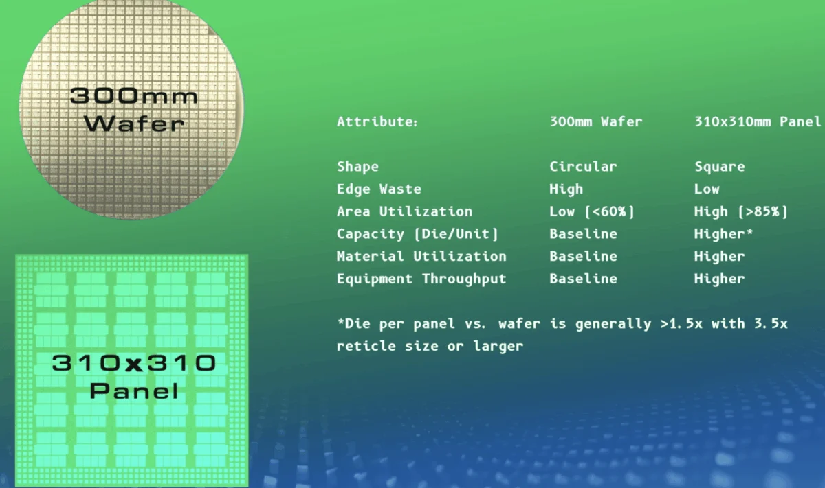
At the heart of the ECTC discussions was the transition from wafer-level packaging to panel-level packaging (PLP). This shift is driven by the need for greater economies of scale and higher throughput. ASE, a global leader in assembly and test services, showcased its latest progress in automated panel-level packaging lines. By utilizing a 310mm x 310mm format, the industry can significantly increase the number of chips processed in a single batch compared to traditional 300mm circular wafers. The larger surface area of a rectangular panel allows for better utilization of space, reducing the "kerf" or wasted area inherent in circular substrates.
Complementing the move to panels is the maturation of hybrid bonding. This technology enables the direct connection of copper-to-copper pads between stacked dies without the need for traditional solder bumps. At ECTC, experts highlighted how hybrid bonding is reaching pitch sizes below 10 microns, a necessity for the next generation of High Bandwidth Memory (HBM4) and complex Chip-on-Wafer-on-Substrate (CoWoS) architectures. The elimination of solder bumps reduces parasitic capacitance and resistance, leading to faster signal transmission and lower power consumption—critical factors for AI data centers where energy costs are a primary concern.
Memory Architecture and the AI PC Revolution
While packaging took center stage at ECTC, the broader industry saw significant product announcements aimed at the burgeoning AI PC market. Rambus introduced a comprehensive DDR5 9600 client memory module chipset designed for high-performance CUDIMM (Clocked Unbuffered Dual In-line Memory Module) and CSODIMM (Clocked Small Outline Dual In-line Memory Module) formats. As AI workloads migrate from the cloud to the edge, the demand for local memory bandwidth has skyrocketed. The DDR5 9600 chipset represents a significant leap in data transfer rates, enabling laptops and desktop workstations to handle complex large language models (LLMs) with reduced latency.
Intel also made waves by announcing a new family of processors specifically optimized for handheld gaming systems. These devices, which require a delicate balance of high-performance graphics and strict thermal management, benefit directly from Intel’s advanced interconnect technologies. In a retrospective discussion at the event, Intel engineers detailed the origins and evolution of the Embedded Multi-die Interconnect Bridge (EMIB). EMIB has become a foundational technology for Intel’s "tiles" or chiplets, allowing different silicon nodes to be integrated into a single package with high-speed, low-latency links. This modular approach is now the standard for Intel’s roadmap, spanning from consumer gaming to enterprise-grade Xeon processors.
Engineering Design and AI-Driven Simulation
The complexity of modern chip design has reached a point where traditional simulation methods are often too slow to keep pace with rapid development cycles. To address this, Siemens and Keysight introduced AI-integrated tools designed to streamline the design-to-validation pipeline. Siemens expanded its Simcenter portfolio by adding geometric deep learning technology. This "PhysicsAI" capability allows engineers to explore "what-if" scenarios in real-time, creating efficient reduced-order models from computational fluid dynamics (CFD) simulation data. This shift from physics-based simulation to AI-augmented prediction can reduce simulation times from days to minutes, allowing for more thorough thermal and structural optimization of advanced packages.
Keysight Technologies addressed the widening semiconductor talent gap by introducing an "executable whiteboard" within its RF circuit simulation software. This tool captures the entire decision-making process of a design, including optimizations and parameters, and transforms it into structured data ready for AI workflows. By digitizing the tribal knowledge of senior engineers, these tools help junior designers navigate the complexities of radio frequency (RF) and high-speed digital design, ensuring that validation reaches its limits without compromising project timelines.
Innovations in Materials and Secure Payment Solutions
Materials science remains the bedrock of semiconductor progress. Lintec, a prominent adhesives and materials firm, announced the establishment of a new center within Japan’s National Institute of Advanced Industrial Science and Technology. The center will focus on the production of carbon nanotube (CNT) EUV pellicles. As Extreme Ultraviolet (EUV) lithography becomes standard for sub-5nm nodes, protecting expensive photomasks from contamination is vital. CNT-based pellicles offer superior transparency and thermal resistance compared to traditional silicon-based versions, ensuring high yields in high-volume manufacturing.
In the consumer electronics space, Infineon released SECORA Connect X, an all-in-one payment solution designed to turn smart wearables into secure contactless payment devices. This ready-to-integrate solution is aimed at the growing market for smart rings, fitness trackers, and watches. By miniaturizing the secure element and antenna requirements, Infineon enables OEMs to offer financial transaction capabilities in increasingly smaller form factors without sacrificing security or battery life.

Research Breakthroughs: From Deep Space to Monolithic 3D
The academic contributions at ECTC and concurrent research announcements highlighted the future of silicon beyond the current five-year roadmap. Researchers at Georgia Tech revealed a breakthrough in memory for extreme environments. They discovered that NAND flash memory constructed with ferroelectric materials can withstand radiation levels up to 30 times higher than conventional NAND. This discovery has profound implications for deep space missions and satellite technology, where cosmic radiation typically limits the lifespan and reliability of electronic components.
Closer to home, the University of Illinois Urbana-Champaign (UIUC) demonstrated a low-temperature technique for stacking single-crystal silicon transistor layers. This enables the creation of monolithic 3D chips—vertical integration where layers are built directly on top of one another rather than being bonded after fabrication. By staying within the "back-end" thermal limits (the maximum temperature the existing metal layers can withstand), UIUC researchers have paved the way for dense vertical integration that could theoretically triple the transistor density of a standard chip without increasing its footprint.
In the field of photonics, a team led by Monash University announced the creation of an on-chip programmable valley optoelectronic nanocircuit. By integrating chirality-selective meta-waveguide photodetectors with transition metal dichalcogenides (TMDs), the researchers have developed a circuit that can manipulate the "valley" degree of freedom in electrons. This represents a step toward valleytronics, a potential successor to traditional electronics that uses the position of electrons in a crystal lattice to store and process information with even lower energy requirements.
Security Standards and the Post-Quantum Era
As the industry prepares for the era of quantum computing, the security of existing silicon designs has come under scrutiny. GlobalPlatform, a leading security standards consortium, launched "Pavona," an open-source silicon distribution for secure-by-default chip designs. Pavona includes certification-ready intellectual property (IP) and two reference designs already taped out on TSMC’s 3nm process. Notably, the project includes what is described as the first openly available Post-Quantum Cryptography (PQC) stack for embedded silicon. With founding members including Qualcomm, Oxford University, and the Max Planck Institute, Pavona aims to provide a standardized, transparent foundation for the next generation of Root of Trust (RoT) designs, ensuring that devices remain secure even against quantum-based attacks.
Chronology of Industry Events and Future Outlook
The developments at ECTC are part of a broader sequence of industry milestones scheduled for the summer of 2026. Following the conclusion of ECTC on May 29, the industry will pivot to COMPUTEX Taipei (June 2–5), where the focus is expected to shift toward consumer hardware and AI integration in the PC ecosystem. This will be followed by the IEEE/JSAP Symposium on VLSI Technology and Circuits in Honolulu (June 14–18), which typically dives deeper into the transistor-level physics and circuit design breakthroughs that will power the products of 2028 and beyond.
The collective announcements this week signal a clear trend: the "center of gravity" in semiconductor innovation has moved to the package. As monolithic chips become prohibitively expensive to design and manufacture at the bleeding edge, the ability to mix and match chiplets from different vendors, connected via fine-pitch interconnects on large-scale panels, will define the winners of the AI era. The integration of AI into the design tools themselves further accelerates this cycle, creating a feedback loop where silicon designed for AI is used to design even more efficient AI silicon.
Broad Impact and Economic Implications
The move toward advanced packaging and panel-level processing is not merely a technical triumph but an economic necessity. As the cost per transistor on a monolithic die begins to plateau, the industry must find new ways to deliver the performance-per-watt improvements that customers demand. The adoption of 310mm x 310mm panels, as advocated by ASE and others, represents a significant capital expenditure for OSATs (Outsourced Semiconductor Assembly and Test) but promises long-term cost reductions that will make high-end AI hardware more accessible.
Furthermore, the focus on workforce development and "executable whiteboards" highlights a critical bottleneck: the human element. With the global semiconductor industry projected to become a trillion-dollar market by 2030, the shortage of skilled design and packaging engineers remains a top-tier risk. The tools and standards introduced this week, from Siemens’ AI simulation to GlobalPlatform’s open-source security, are essential components of an infrastructure designed to sustain growth in a highly competitive and geopolitically sensitive landscape.
As the ECTC concludes, the industry leaves Orlando with a reinforced consensus: the future is modular, vertically integrated, and increasingly defined by the materials and connections that surround the silicon. The transition to HBM4, the rise of glass substrates, and the deployment of post-quantum security are no longer distant prospects—they are the immediate milestones of a rapidly accelerating roadmap.
