
The electronics industry is currently grappling with a fundamental shift in how printed circuit boards (PCBs) are designed, verified, and brought to market. As high-speed digital protocols and increasing component densities push traditional manufacturing limits, the historical reliance on manual visual inspection for electrical sign-off has become a primary bottleneck in hardware development. Traditionally, electrical verification is a tedious, manual process that, due to time constraints, is often performed only once at the final stage of the design cycle. This "wait-and-see" approach frequently results in the discovery of critical errors—such as signal integrity (SI) failures or electromagnetic interference (EMI) violations—only after the layout is supposedly complete. When these issues are identified late, designers are forced into costly and time-consuming "respins," redoing component placement and trace routing, which triggers additional sign-off cycles and cascades into significant project delays.

To mitigate these risks, the industry is moving toward an automated rule-verification process implemented throughout the entire PCB layout design cycle. This methodology, often referred to as "shifting left," incorporates signal integrity, power integrity (PI), EMI, and high-voltage safety rules directly into the design workflow. By utilizing built-in electrical parameters, 2D field solvers, and vendor-specific IBIS (Input/Output Buffer Information Specification) models, hardware engineers can now run sophisticated electrical rules early and often. This automated check-and-correct approach ensures that electrical protocols are adhered to from the first trace, providing hardware engineers with greater confidence and reducing the reliance on a single, high-stakes final review.
The Evolution of Hardware Design Complexity
The challenges facing modern hardware designers are rooted in two decades of rapid technological evolution. In the late 1990s and early 2000s, PCB design was primarily concerned with basic connectivity and rudimentary spacing rules. However, the universal adoption of high-speed protocols such as Universal Serial Bus (USB), Peripheral Component Interconnect Express (PCIe), Double-Data Rate (DDR) memory, and High-Definition Multimedia Interface (HDMI) has fundamentally changed the landscape.

The trajectory of DDR memory serves as a prime example of this escalating complexity. When DDR was introduced in 1998, it operated at relatively modest clock speeds. By the time DDR4 became the industry standard, data rates had climbed to 3200 MT/s. The upcoming DDR6 standard, expected to be finalized by the Joint Electron Device Engineering Council (JEDEC) around 2027, is anticipated to push speeds even further, potentially reaching 17.6 Gbps or higher. Each generation of these protocols introduces stricter timing margins, more complex impedance requirements, and heightened sensitivity to crosstalk and noise.
As these standards evolve, hardware designers are no longer generalists. The sheer volume of technical specifications has forced a transition toward extreme specialization. It is now common for engineering teams to have dedicated DDR experts, SerDes (Serializer/Deserializer) specialists, and EMI consultants. While this specialization ensures deep expertise, it also creates organizational silos. If a design team must wait for a specific expert to perform a manual review of every high-speed net, the design release timeline becomes tethered to that expert’s availability. This creates a significant drag on time-to-market, which in modern electronics can be the difference between a product’s success and its obsolescence.

The Hidden Costs of Disparate Tool Flows
One of the most significant hurdles in the current PCB verification landscape is the fragmented nature of simulation and modeling tools. Experts in signal and power integrity often spend the majority of their time not on actual analysis, but on the acquisition and preparation of models. These models range from simple datasheet parameters to highly complex S-parameters and 3D meshed structures.
In many design environments, the tools used for validation are "point tools"—software designed to solve one specific problem with high precision but lacking integration with the broader design ecosystem. A specialist might use one vendor’s simulator for power integrity and another’s for thermal analysis. Because these tools often do not "talk" to one another, the results must be stitched together manually. This manual data handling is not only time-consuming but also introduces a high probability of human error.

Industry data suggests that the "ease-of-use" of a tool is just as critical as its technical capability. As modeling complexity increases, the tool must remain accessible to the layout designer, not just the PhD-level simulation expert. The goal of modern Electronic Design Automation (EDA) is to automate the "easy" problems—the repetitive, rule-based checks—thereby freeing up specialists to focus on the truly unique and difficult simulation challenges that could cause a catastrophic board failure.
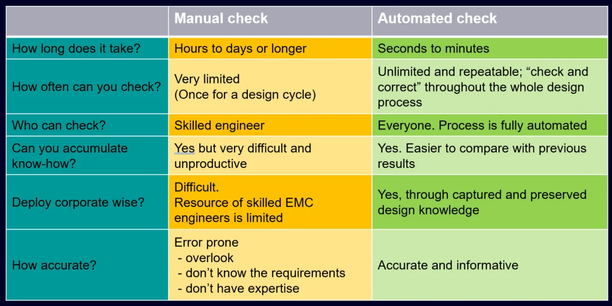
Manual vs. Automated Inspection: A Comparative Analysis
The traditional manual inspection of a PCB is a grueling process. An expert reviewer must go layer by layer and net by net, visually checking for potential pitfalls based on their personal knowledge and experience. As boards become denser, the number of items on the "must-check" list grows exponentially.

In a manual workflow, reviewers often have to make difficult trade-offs. Because they cannot possibly simulate or visually inspect every single net on a board with 2,000+ connections, they focus on what they perceive to be the "critical" nets—usually the longest or shortest traces. This leaves a significant portion of the board unverified, operating on the hope that if the corner cases work, the rest of the board will follow suit. However, in high-frequency design, an seemingly insignificant trace can become an unintentional radiator of EMI if it crosses a split in a power plane.
| Feature | Manual Inspection | Automated DRC (e.g., HyperLynx DRC) |
|---|---|---|
| Speed | Hours to days per iteration | Seconds to minutes |
| Consistency | Subject to human fatigue/error | 100% repeatable and objective |
| Scope | Limited to "critical" nets | Full board coverage (every net) |
| Timing | Typically only at the end of design | Throughout the entire design cycle |
| Integration | Requires manual data entry/review | Direct integration with layout data |
For example, a common issue is the "metal island"—isolated copper on a layer that is not tied to any net. In a manual review of an eight-layer board, finding these islands might take an engineer 30 to 60 minutes of tedious toggling between layers. In contrast, automated tools like Siemens’ HyperLynx DRC can identify every isolated copper instance across all layers in a matter of seconds. In one documented case, the automated tool found a specific island and 27 other potentially harmful layout violations in less time than it took the designer to open the manual checklist.

Technical Deep Dive: EMI and Plane Transitions
Electromagnetic interference is often called the "black magic" of PCB design because it is notoriously difficult to detect via traditional simulation. Many EMI issues are caused by subtle layout flaws, such as inductance loops created by breaks in return current paths.
A critical rule in high-speed design involves vertical reference plane changes. When a signal transitions from one layer to another through a via, its return current must also find a path to transition between reference planes. If the reference planes are at different potentials (e.g., one is Ground and the other is Power), a decoupling capacitor or a stitching via must be placed nearby to provide a low-impedance path for the return current.

Traditional layout DRCs usually only check for physical spacing—ensuring a via doesn’t hit a trace. They do not understand the electrical relationship between a signal via and its return path. Automated electrical DRCs, however, can explicitly check for the distance to the nearest stitching component. They can even incorporate IBIS models to factor in the specific edge rates (rise and fall times) of the signal. A faster edge rate requires a much closer stitching via to prevent common-mode radiation. Identifying these issues manually is nearly impossible in a dense layout, but an automated rule can flag a violation and provide specific layout advice in under a minute.
Another frequent culprit for signal degradation is the "nets crossing gaps" violation. When a high-speed trace crosses a split in a power or ground plane, it experiences an immediate change in impedance. This causes signal reflections and creates an EMI "antenna." While a designer might visually spot a major trace crossing a gap, automated tools can scan the entire board for every instance of this, factoring in the gap size and the proximity of nearby stitching capacitors that might mitigate the effect.

Power Integrity and the Future of EDA
Ensuring stable power delivery to high-performance ICs is the other half of the electrical verification equation. Modern processors and FPGAs operate at low voltages with extremely high current demands, making them highly sensitive to voltage drops and AC noise.
Out-of-the-box power integrity rules in tools like HyperLynx DRC allow designers to verify decoupling capacitor placement and coverage. Unlike traditional DRCs that look at simple Euclidean distance, electrical DRCs can calculate the actual "routed length" from an IC power pin to its decoupling cap, including the parasitic inductance of the ground nets. This ensures that the capacitors are actually effective at the frequencies the IC is operating at. If a decoupling capacitor is placed too far away, the entire design might fail AC analysis, leading to intermittent system crashes that are incredibly difficult to debug in the field.

Strategic Implications and Industry Impact
The move toward automated, rule-based verification represents a fundamental change in the economics of hardware development. The cost of a PCB respin is not merely the cost of the raw materials and fabrication; it is the cost of engineering hours, the cost of delayed testing, and the opportunity cost of a late product launch. For high-volume consumer electronics, a one-month delay can result in millions of dollars in lost revenue.
By empowering layout designers to perform their own high-level electrical checks, companies can optimize their most expensive resource: the signal and power integrity experts. These specialists are no longer bogged down by "low-level" checks like finding metal islands or checking decoupling cap distances. Instead, they can focus on complex 3D electromagnetic modeling and system-level simulations that define the next generation of technology.

Furthermore, as the industry moves toward more collaborative and globalized design chains, automated DRCs provide a standardized "language" of quality. A third-party layout house can run a standardized suite of rules provided by the client, ensuring that the design meets the client’s electrical standards before the files are even handed over. This provides a level of "peace of mind" that manual inspection simply cannot offer.
In conclusion, the complexity of modern electronics has outpaced the capabilities of manual PCB verification. The adoption of automated, electrical rule-based sign-off is no longer a luxury but a necessity for teams working with high-speed protocols and dense architectures. Tools like HyperLynx DRC from Siemens EDA, which offer over 100 pre-defined rules spanning SI, PI, and EMI, are setting a new standard for design efficiency. By integrating these checks throughout the design cycle, hardware engineers can ensure that their products are not only physically manufacturable but electrically sound, significantly reducing the risk of costly respins and accelerating the path to market.
