
The rapid evolution of generative artificial intelligence and Large Language Models (LLMs) has brought the semiconductor industry to a critical crossroads regarding memory architecture. As models grow to encompass hundreds of billions, and eventually trillions, of parameters, the traditional methods of storing and retrieving these "weights" have become a primary bottleneck in system performance. To address this "memory wall," Sandisk, in collaboration with SK Hynix, has proposed a new standard known as High Bandwidth Flash (HBF). This technology aims to place massive amounts of non-volatile memory directly within the GPU or accelerator package, providing a high-capacity, high-speed alternative to traditional storage and a necessary complement to High Bandwidth Memory (HBM).
The Emergence of High Bandwidth Flash
Announced in early 2025, High Bandwidth Flash represents a paradigm shift in how data centers handle AI inference workloads. While HBM has become the gold standard for high-speed volatile memory, its capacity remains limited and its cost high. Current HBM3e and upcoming HBM4 stacks offer capacities in the range of 24 GB to 36 GB per cube, which, even when clustered around a GPU, often fall short of the requirements for the largest LLMs without significant off-chip communication.
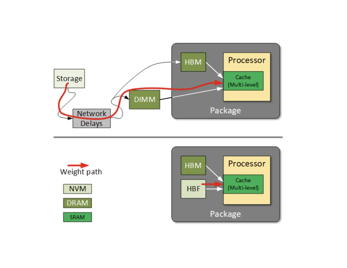
HBF is designed to fill the gap between HBM and traditional Solid State Drives (SSDs). By utilizing a 16-die-plus-base-die flash stack, HBF achieves a physical footprint identical to HBM, allowing it to be co-packaged with processors using advanced packaging techniques. However, unlike HBM, which is based on DRAM technology, HBF utilizes NAND flash. This allows for significantly higher density; where a state-of-the-art HBM stack might hold 192 GB to 400 GB in the near future, HBF is already targeting capacities of 3 Terabits (Tb) or approximately 512 GB per stack in its initial generation.
Xi-Wei Lin, executive director of applications engineering at Synopsys, noted that HBF was specifically engineered to utilize flash for high-bandwidth, high-capacity memory, targeting the unique demands of AI inference. By keeping model parameters inside the package, HBF eliminates the need for data to traverse the relatively slow PCIe bus or network-attached storage, thereby reducing latency and energy consumption.
Architectural Innovation: Separating Activations from Weights
To understand the necessity of HBF, it is essential to distinguish between the two types of data processed during AI workloads: activations and weights.
Activations are the dynamic data sets consisting of inputs to the model and the intermediate results generated by each computational layer. Because these values change constantly during a processing run, they require the high-speed, high-endurance write capabilities of SRAM or DRAM (HBM). Weights, or parameters, are the pre-calculated values that define the model’s intelligence. During the inference phase—when a model is being used to generate a response rather than being trained—these weights are static.
The industry has long struggled with where to store these weights. Keeping them in SRAM is impossible due to size constraints. Storing them in HBM is efficient but expensive and capacity-limited. Moving them from an external SSD to the processor creates a massive latency penalty. HBF proposes a middle ground: storing the static weights in high-density flash right next to the processing cores.
"HBF is an architectural stage that bridges the gap between high-bandwidth access and high storage footprint," said Sharad Chole, chief scientist and co-founder at Expedera. Chole explained that by connecting these flash stacks directly to the accelerator, designers can move away from the limitations of PCIe speeds and latencies, allowing AI workloads to address storage with the same ease they currently address DDR memory.
Technical Specifications and Performance Metrics
The proposed HBF standard introduces several key performance benchmarks that distinguish it from existing memory tiers. The first generation of HBF is expected to offer a read bandwidth of 1.6 TB/s, matching the physical height and power profile of HBM4. This ensures that system architects can integrate HBF into existing design flows without radical changes to the thermal or mechanical constraints of the GPU package.
According to data released by Sandisk, the roadmap for HBF suggests aggressive scaling in capacity and efficiency:
- Generation 1: Baseline capacity (512 GB per stack) and read bandwidth (1.6 TB/s).
- Generation 2: 1.5x increase in capacity and 1.45x increase in read bandwidth, with a 20% reduction in energy consumption.
- Generation 3: 2x increase in capacity and 2x increase in read bandwidth compared to Gen 1, with energy consumption reduced to 64% of the original baseline.
The technology leverages multi-array parallelism and a re-architected internal read path to minimize fetch latency. Cynthia Hsu, senior director of flash memory design at Sandisk, emphasized that HBF is not merely a new interface but a systemic redesign. "It involves re-architecting the internal read path and leveraging multi-array parallelism more intelligently so data can be accessed and delivered with lower effective latency and more consistent bandwidth," Hsu stated.
The Challenge of Flash Physics: Why Inference is the Target
Despite its capacity advantages, NAND flash faces inherent physical limitations that prevent it from replacing HBM entirely. The primary hurdle is write speed. Writing to flash involves complex quantum mechanical processes, including Fowler-Nordheim tunneling or hot-carrier injection, which are significantly slower than the charge-based storage used in DRAM. Furthermore, flash cells must be erased before they can be rewritten, a process that occurs in large blocks and introduces further delays.
"Flash is designed to be as cheap as it can possibly be, and because of that, it does give up some speed," observed Jim Handy, memory analyst at Objective Analysis. Handy noted that while the read speeds can be optimized to be highly competitive, the write cycle remains a bottleneck.

This physical reality dictates that HBF is currently suitable for inference, not training. During the training of an AI model, weights are updated constantly as the system learns, requiring high-speed write endurance. During inference, however, the weights are read-only. This makes HBF the ideal repository for the "frozen" parameters of a deployed model.
Additionally, flash endurance—the number of times a cell can be written to before failing—remains a concern. While high-end enterprise flash can handle thousands of write cycles, this is orders of magnitude lower than the near-infinite endurance of DRAM. However, for inference applications where the model is loaded once and read millions of times, endurance is a negligible factor.
Standardization and the Role of the Open Compute Project (OCP)
In a strategic move, Sandisk and SK Hynix have submitted the HBF technology to the Open Compute Project (OCP) for standardization, rather than the more traditional JEDEC (Joint Electron Device Engineering Council). This decision reflects the urgent pace of the AI market.
Cynthia Hsu explained that OCP was chosen because its working groups are "highly goal-oriented," allowing for real-time iteration on specifications. This speed is critical for matching the rapid innovation cycles of AI hardware. The standardization effort is supported by a Memorandum of Understanding (MoU) between Sandisk and SK Hynix, intended to encourage a broader ecosystem of vendors to adopt the HBF protocol.
Standardization is vital because HBF requires a different interface protocol than HBM. For the technology to proliferate, GPU manufacturers like NVIDIA, AMD, and Intel, as well as AI ASIC startups, must design their memory controllers to support the HBF interface.
Comparison with Alternative Non-Volatile Memories
While HBF utilizes established NAND flash technology, the industry continues to explore other Non-Volatile Memory (NVM) types, such as Magnetoresistive RAM (MRAM) and Resistive RAM (RRAM).
MRAM offers much higher endurance and faster write speeds than NAND, but it faces a difficult trade-off: cells are typically optimized for either speed or data retention, but rarely both at the scale required for AI. RRAM, while promising, has struggled with manufacturing maturity and cost-competitiveness.
Sandisk’s decision to stick with NAND for HBF is rooted in pragmatism. "High Bandwidth Flash is built around the strengths of NAND—density, scalability, and cost efficiency—using a technology foundation that’s proven and available today," Hsu said. By leveraging the massive existing infrastructure for NAND production, HBF can achieve price points that newer NVM technologies cannot yet match.
Future Chronology and Market Impact
The timeline for HBF deployment is aggressive, reflecting the industry’s hunger for memory solutions. Sandisk plans to provide the first samples of HBF in the second half of 2026. If the sampling process is successful, the first AI inference devices utilizing HBF are expected to reach the market in early 2027.
The impact of this technology on data center architecture could be profound. Currently, scaling an LLM often requires "model splitting," where a single model is distributed across multiple GPUs because its parameters cannot fit into the memory of a single card. This introduces significant "tail latency" as different parts of the model communicate over a network. With HBF, a single GPU could potentially hold a much larger model—or even multiple models—entirely within its own package.
Steven Woo, a fellow and distinguished inventor at Rambus, noted that HBF is gaining attention as system designers look for new memory tiers that sit between DRAM and traditional NAND. By providing 8x to 16x the capacity of HBM at a similar read bandwidth and price point, HBF could significantly lower the Total Cost of Ownership (TCO) for AI service providers.
Conclusion: A New Dimension for AI Architects
The introduction of High Bandwidth Flash represents a maturing of AI hardware design. As the industry moves past the initial rush of the generative AI boom, the focus is shifting toward efficiency, cost-effectiveness, and the ability to run increasingly complex models at scale.
While HBM will remain essential for the high-speed computational "scratchpad" of AI processing, HBF provides the "library" where the vast knowledge of the model can be stored and accessed with minimal delay. By bringing the weights closer to the processor, Sandisk and SK Hynix are not just solving a storage problem; they are providing architects with a new dimension of design that was previously inaccessible. As the 2027 rollout approaches, the semiconductor industry will be watching closely to see if HBF can do for AI inference what HBM did for AI training: break through the memory wall and enable the next generation of machine intelligence.
