
The semiconductor industry is currently navigating a paradigm shift in advanced packaging, moving away from traditional microbumps toward bumpless hybrid bonding. This transition allows for unprecedented signal pitch, but as connections shrink to 1µm and below, the sheer volume of interconnects—reaching into the billions per chip—is forcing a complete overhaul of how engineers approach yield management, process uniformity, and electrical verification. When a single package can contain more connections than there are people on several continents, the industry can no longer rely on individual inspection or traditional testing methodologies. Instead, the focus has shifted toward architectural modularity, built-in redundancy, and a manufacturing precision that mirrors the exactitude of atomic-level engineering.
The Mathematical Reality of the Billion-Connection Era
The move to a 1µm pitch is the primary catalyst for the explosion in connection density. In traditional flip-chip packaging, microbumps typically operate at a 30µm to 40µm pitch. By contrast, hybrid bonding eliminates the solder bump entirely, bonding copper pads directly to copper pads within a dielectric field. At a 1µm pitch, a single square millimeter of silicon can theoretically host one million connections.
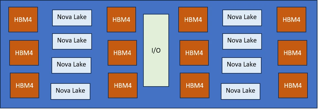
To put this scale into perspective, consider a modern high-performance computing (HPC) or AI accelerator package. A hypothetical processor assembly utilizing eight logic dies (such as those modeled after Intel’s Nova Lake architecture) would feature roughly 97 million connections per die, totaling nearly 800 million for the logic portion alone. When integrating next-generation High Bandwidth Memory (HBM4), which utilizes 16-high stacks, the numbers escalate exponentially. A single 12-stack HBM4 configuration can contribute over 23 billion connections. Combined with the interposer and I/O chiplets, a single high-end package will soon exceed 26.7 billion internal connections.
Industry experts note that even the 1µm pitch is not a physical ceiling. Thomas Pleschke, business development manager at EV Group, suggests that the roadmap points toward 200nm pad pitches. At that density, two 300mm wafers bonded together could theoretically contain several trillion connections. This trajectory makes it mathematically impossible to verify each connection through external metrology or traditional probe testing.
Evolution of Interconnect Technology: A Brief Chronology
The journey to billions of connections has been defined by the industry’s need to overcome the "memory wall" and the limitations of data movement between chips.
- 2010s (The Microbump Era): Scaling focused on shrinking solder bumps. While effective, the height of the bumps and the need for underfill created parasitic capacitance and limited how closely dies could be stacked.
- 2016–2020 (The Rise of Wafer-to-Wafer Bonding): Hybrid bonding first saw high-volume success in CMOS image sensors (CIS). Because these sensors required simple, repetitive connections, they provided the perfect sandbox for perfecting the copper-to-copper bonding process.
- 2021–2023 (Logic Integration): The introduction of technologies like AMD’s 3D V-Cache, utilizing TSMC’s SoIC (System on Integrated Chips) technology, marked the first major application of hybrid bonding in high-performance logic.
- 2024–2026 (The HBM4 Transition): The industry is currently preparing for HBM4, where hybrid bonding will become essential to keep stack heights manageable while providing the massive bit-width required for AI training.
- 2027 and Beyond (Sub-Micron Scaling): The roadmap moves toward "bumpless" architectures at 500nm to 200nm pitches, necessitating new materials and hexagonal pad layouts to maintain uniformity.
Manufacturing Precision: The "Rainfall" Challenge
For a billion-connection chip to achieve viable yield, the manufacturing process must exhibit near-perfect uniformity across the entire 300mm wafer. Hybrid bonding requires surfaces to be pristine; even a single nanometer of unintended roughness can prevent the atomic-level bonding required for a reliable connection.
Chee Ping Lee, managing director for advanced packaging at Lam Research, describes the required precision through a vivid analogy: "It is like creating rainfall uniformly over the entirety of the United States with such precision that buckets placed one meter apart fill at exactly the same rate."
The process involves several critical steps that must be executed in parallel at a wafer scale. Dielectric deposition provides the initial bond, followed by plasma drilling to create holes with highly repeatable sidewall profiles. Finally, billions of holes are filled with copper simultaneously. A critical challenge during the Chemical Mechanical Polishing (CMP) phase is "copper dishing." The copper must be recessed by exactly 3 to 5nm so that when the wafers are heated, the copper expands just enough to create a solid metallic bond after the surrounding dielectric has already fused.
Material Science and Signal Integrity
As pitches shrink, the dielectric material separating the copper pads becomes a focal point for reliability. When I/O density increases by an order of magnitude, the physical distance between conductors decreases, raising the risk of signal interference and copper diffusion.
To maintain signal integrity at high frequencies, materials with low dielectric constants (low-k) are preferred. However, there is a technical trade-off. Standard Silicon Dioxide (SiO2) has a dielectric constant of roughly 3.9 to 4.2. To prevent copper from migrating through the material—a phenomenon that can cause short circuits over time—manufacturers often turn to Silicon Nitride (SixNy) or Silicon Carbon Nitride (SiCN). While these materials are better at blocking copper diffusion, they have higher dielectric constants (ranging from 4.0 to 9.0), which can negatively impact signal speed and power consumption.
Furthermore, thinner wafers are required to reduce the signal path and overall package height. Amit Kumar, applications engineer at Brewer Science, notes that wafers are being ground down to tens of microns. This "ultra-thinning" requires temporary bonding materials that can withstand the mechanical and thermal stress of multiple stacking cycles while maintaining a total thickness variation (TTV) that is virtually zero.
The Shift from Physical Inspection to Built-In Self-Test (BiST)
In traditional manufacturing, optical inspection tools can identify defects in solder bumps. However, hybrid bonds are buried between two layers of silicon, and their size is often smaller than the wavelengths of light used in high-speed optical inspection. Lakshmi Jain, director of product marketing at Synopsys, points out that defects at these densities are often electrical rather than visual, appearing as "weak" bonds or small clusters of failures.
Since physical inspection is impractical, the industry is pivoting toward architectural solutions. The most prominent of these is the use of Built-In Self-Test (BiST) engines embedded directly into the chip’s I/O library.
One emerging strategy is the "cluster-based" architecture. Instead of treating billions of connections as a single monolithic block, I/Os are grouped into repeatable clusters. For example, Synopsys’s 3DIO IP groups interconnects into 16-lane clusters, each with its own clock tree, power management, and, most importantly, its own BiST engine. This allows the chip to test itself both before and after the bonding process.
Redundancy, Repair, and Yield Recovery
In a system with billions of connections, the statistical probability of a perfect die is low. To combat this, designers are incorporating redundancy and repair mechanisms. If a BiST engine identifies a defective lane within a cluster, the system can "remap" the signal to a spare redundant pad.
This approach transforms the yield equation. Rather than discarding a complex die due to a single failed bond among a billion, the architecture "tolerates" the imperfection. The amount of redundancy required is a delicate balance; too little redundancy leads to failed chips, while too much redundancy wastes valuable silicon real estate. According to Jain, the specific redundancy ratio depends heavily on the foundry’s defect characteristics and the specific process technology being used.
Broader Impact and Industry Implications
The transition to billion-connection hybrid bonding has implications that extend far beyond the cleanroom. It represents a fundamental shift in the semiconductor value chain, requiring closer collaboration between EDA (Electronic Design Automation) tool providers, equipment manufacturers, and material scientists.
- Reliability Improvements: Surprisingly, despite the complexity, hybrid bonding can improve long-term reliability. Copper-to-copper connections exhibit lower resistance and capacitance than traditional microbumps, leading to a lower Bit Error Rate (BER). This intrinsic reliability is critical for the scaling of AI fabrics, where data integrity is paramount.
- Power Efficiency: By enabling shorter interconnects and eliminating the need for high-power I/O drivers required for longer traces, hybrid bonding significantly reduces the "energy per bit" moved across the package.
- Thermal Management: The elimination of solder bumps and the use of direct silicon-to-silicon bonding improves the thermal conductivity of the stack, allowing for better heat dissipation in high-performance 3D-stacked chips.
As the industry moves toward 200nm pitches and trillion-connection wafers, the challenges will only intensify. The success of the next generation of computing—from autonomous systems to generative AI—will depend on the ability to build, test, and repair these massive interconnect fabrics with a level of automation and precision that was once considered the realm of science fiction. The era of managing individual interconnects is over; the era of architectural resilience has begun.
