

The rapid proliferation of artificial intelligence across diverse sectors—from the pursuit of artificial general intelligence (AGI) to breakthroughs in pharmaceutical drug discovery and advanced materials science—has fundamentally transformed the hierarchy of semiconductor design priorities. In the previous era of computing, the primary metric of success was the development of the fastest possible processor at the smallest available process node. However, the industry is currently undergoing a paradigm shift where the focus is moving away from raw compute power toward the architecture of holistic systems designed for the rapid, deterministic movement of massive data volumes. As processors move toward 18-angstrom nodes and beyond, the industry faces a sobering reality: even the most sophisticated silicon is rendered ineffective if it remains idle, waiting for data to be retrieved from memory or navigating congested data pathways.
The Shift from Chip-Centric to System-Centric Design
Modern high-performance computing (HPC) environments now require a delicate balance across three core pillars: processing units, memory subsystems, and interconnects. This balance is not merely a matter of bandwidth but of sophisticated orchestration. To prevent "data starvation," where high-speed processors sit underutilized, architects must ensure that data arrives at the execution unit precisely when needed.
Industry experts emphasize that the nature of the interaction—such as the real-time responsiveness required by AI chatbots—changes the fundamental requirements for network and I/O (Input/Output) connectivity. Deterministic, low-latency communication is no longer a luxury but a requirement for the commercial viability of AI products. This shift has necessitated a move toward multi-die assemblies and advanced packaging techniques, which, while solving density issues, have introduced a complex web of design trade-offs involving signal integrity, thermal management, and power delivery.
A Chronology of Interconnect Evolution
To understand the current state of I/O design, it is necessary to trace the evolution of computing architecture over the last two decades.
- The Multi-Core Era (Pre-2012): During this period, scaling was achieved by integrating multiple cores within a single monolithic processor. Communication was largely internal to the silicon, managed by traditional on-chip buses.
- The Server Scaling Era (2012–2022): The focus shifted to increasing throughput by packing multiple processors into a single server rack. Interconnects like PCIe (Peripheral Component Interconnect Express) became the standard for connecting CPUs to peripheral accelerators.
- The Generative AI Revolution (2023–Present): The emergence of Large Language Models (LLMs) and unstructured data processing revealed that traditional CPU-centric architectures were insufficient. This led to the rise of workload-specific accelerators (GPUs and TPUs) and the need for a unified compute facility where thousands of chips act as a single, cohesive computer.
In this current phase, the "scaling laws" of AI dictate that the quantity of data and the efficiency of its movement are the primary drivers of model intelligence. This has pushed interconnect technology into the realm of 1.6 Terabits per second (Tbps) interoperability, utilizing standards such as Ultra Ethernet and UALink.
The Physics of Integration: Where Economics and Engineering Collide
The transition to chiplets and 3D multi-die packaging represents the most significant challenge in contemporary I/O design. By shortening the physical distance between components, advanced packaging reduces latency; however, it simultaneously multiplies the number of interfaces that must be managed. Engineers are now forced to confront the "nastiest" problems where physics and integration economics collide.
Heterogeneous integration—combining different dies from different process nodes (e.g., a compute die on N2, I/O on N5, and SRAM on N3)—creates a "bookkeeping nightmare" for designers. Each die comes with its own Process Design Kit (PDK), reliability model, and thermal coefficient. Ensuring these disparate elements produce a coherent picture under a heavy AI workload often results in months of design delays.
Furthermore, physical constraints such as thermal gradients and mechanical strain are now bidirectional problems. For instance, high-speed links running at 64 giga-transfers per second are connected via micro-bumps whose impedance can shift based on temperature fluctuations. In 3D-stacked architectures, a "buried" base die may have no direct path to extract heat, creating thermal bottlenecks that can throttle the entire system’s performance.
Reliability, Redundancy, and the Silicon Lifecycle
In the context of hyperscale data centers, I/O failure is not merely a technical glitch; it is a significant financial liability. As clusters grow to include tens of thousands of GPUs, the statistical probability of a link failure increases exponentially. This has elevated "Silicon Lifecycle Management" (SLM) from a secondary consideration to a mandatory design requirement.

To combat these risks, architects are implementing several layers of redundancy:
- Physical Redundancy: The inclusion of extra links in UCIe (Universal Chiplet Interconnect Express) and 3D hybrid bonds to replace failed connections during assembly or after years of field use.
- Protocol-Level Resilience: The adoption of mechanisms like Link Layer Retry (LLR) by the Ultra Ethernet Consortium, which allows for retransmissions at Layer 2, minimizing the latency penalties associated with higher-layer protocols like TCP.
- Telemetry and Sensing: The integration of on-chip sensors to monitor process, voltage, and temperature (PVT) in real-time. This data is aggregated to allow software to predict and repair links before they cause a system-wide crash.
The Open Compute Project (OCP) has recently been instrumental in standardizing these reliability protocols. The introduction of the Multipath Reliable Connection (MRC) protocol allows for data to be "sprayed" across multiple paths, eliminating flow collisions and ensuring that a single link failure does not bring down an entire AI training job.
The "Cluster-as-a-Computer" Philosophy
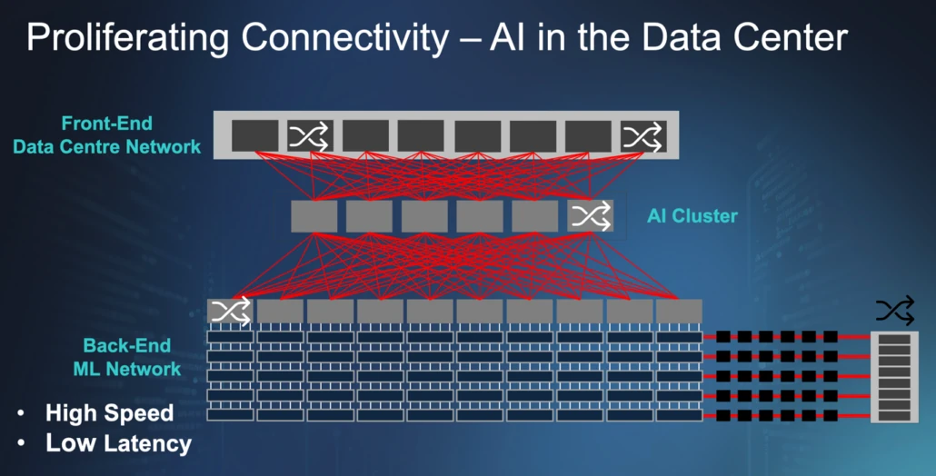
The ultimate goal of modern AI infrastructure is to make a massive cluster of compute nodes operate with the seamlessness of a single processor. This requires "escaping the chip"—maximizing the bandwidth available at the "beachfront" (the edge of the die) to allow chips to talk to one another at speeds comparable to internal on-chip communication.
NVIDIA’s Blackwell NVL72 system serves as a primary case study for this philosophy. By utilizing NVLink and specialized NV switches, the system allows 72 GPUs to act as one giant unit. This "rack-scale design" acknowledges that compute is no longer the sole limitation; rather, the bottleneck has moved to the fabric that binds the GPUs together.
From a chip architect’s perspective, this level of clustering introduces four practical concerns:

- Global Addressability: Can every node see every piece of memory in the cluster?
- Cache Coherency: How do we maintain data consistency across thousands of separate caches?
- Congestion Management: How do we handle "bursty" traffic patterns generated by AI inference without dropping packets?
- Power Budgeting: How is energy apportioned from the data center level down to the individual I/O pins?
Implications for the Semiconductor Industry
The shift toward interconnect-dominated design is reshaping the competitive landscape of the semiconductor industry. Success is no longer determined solely by who has the best transistor technology, but by who can build the most efficient "data highway."
This has led to a surge in demand for EDA (Electronic Design Automation) tools that incorporate "Agentic AI"—AI-driven assistants that help human engineers solve complex physics problems like thermal-bandwidth trade-offs. While these tools are still maturing, they are becoming essential for managing the "multi-dimensional problem" of I/O design.
Moreover, the industry is seeing a move away from monolithic solutions toward disaggregated SoCs (System-on-Chips). While disaggregation introduces latencies and additional power bonds, it offers the flexibility to swap out compute dies while retaining expensive I/O and memory components. This modularity is seen as the only sustainable way to keep pace with the rapid evolution of AI models.
Conclusion: The Multi-Dimensional Frontier
The competition to deliver lightning-fast, accurate AI capabilities is driving the semiconductor industry into a new frontier of system-level design. Architects are no longer just building chips; they are building intricate, balanced ecosystems where every millimeter of routing and every micro-bump of solder is a critical variable in the performance equation.
As AI models continue to grow in scale and complexity, the pressure on I/O and interconnects will only intensify. The winners in this space will be those who can successfully balance the conflicting demands of bandwidth, power, thermal stability, and cost. In the AI era, the "fastest chip" is a misnomer; the true leader is the most interconnected system. The challenge remains to optimize for what is most important to the end user—whether that is the speed of a chatbot’s response or the accuracy of a drug discovery simulation—while navigating the harsh physical and economic realities of modern silicon integration.
